STN1N20
RoHS  RoHS compliant
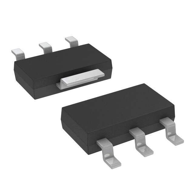
Package TO-261-4, TO-261AA
Category Discrete Semiconductor Products / Transistors - FETs, MOSFETs - Single
Description
MOSFET N-Ch 200 Volt 1 Amp
PDF
/
Buying Options
Total Price: USD $0.27
Unit Price: USD $0.26505
≥1 USD $0.26505
≥10 USD $0.21755
≥100 USD $0.2109
≥500 USD $0.20425
≥1000 USD $0.19665
Inventory: 1747
Minimum: 1
-
+

Technical Details
Compliance
Lead Free Lead Free
RoHS Status ROHS3 Compliant
REACH SVHC No SVHC
Radiation Hardening No
Dimensions
Width 3.5mm
Length 6.5mm
Height 1.8mm
Technical
Nominal Vgs 3 V
Dual Supply Voltage 200V
Drain to Source Breakdown Voltage 200V
Gate to Source Voltage (Vgs) 20V
Threshold Voltage 3V
Continuous Drain Current (ID) 1A
Fall Time (Typ) 5 ns
Vgs (Max) ±20V
Drive Voltage (Max Rds On,Min Rds On) 10V
Rise Time 6ns
Gate Charge (Qg) (Max) @ Vgs 15.7nC @ 10V
Current - Continuous Drain (Id) @ 25°C 1A Tc
Input Capacitance (Ciss) (Max) @ Vds 206pF @ 25V
Vgs(th) (Max) @ Id 5V @ 250μA
Rds On (Max) @ Id, Vgs 1.5 Ω @ 500mA, 10V
Transistor Application SWITCHING
FET Type N-Channel
Turn On Delay Time 6 ns
Case Connection DRAIN
Power Dissipation 2.9W
Operating Mode ENHANCEMENT MODE
Current 1A
Power Dissipation-Max 2.9W Tc
Voltage 200V
Configuration SINGLE WITH BUILT-IN DIODE
Number of Elements 1
JESD-30 Code R-PDSO-G4
Pin Count 4
Base Part Number STN1N
Current Rating 1A
Terminal Form GULL WING
Terminal Position DUAL
Technology MOSFET (Metal Oxide)
Voltage - Rated DC 200V
Subcategory FET General Purpose Power
Terminal Finish Matte Tin (Sn)
Resistance 1.5Ohm
ECCN Code EAR99
Number of Terminations 4
Moisture Sensitivity Level (MSL) 1 (Unlimited)
Part Status Obsolete
Pbfree Code yes
JESD-609 Code e3
Series MESH OVERLAY?
Packaging Tape & Reel (TR)
Operating Temperature -55°C~150°C TJ
Physical
Transistor Element Material SILICON
Number of Pins 3
Package / Case TO-261-4, TO-261AA
Mounting Type Surface Mount
Mount Surface Mount
Alternative Model

Recommended For You

STN1N20+price,STN1N20+datasheet,STN1N20+in stock,buy+STN1N20,finder+STN1N20,STN1N20+tutorials,STN1N20+download