STL8N80K5
RoHS  RoHS compliant
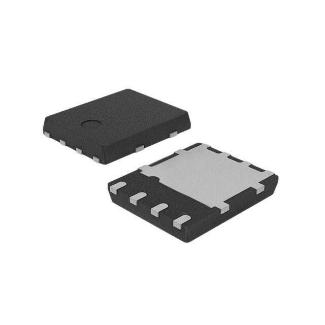
Package 8-PowerVDFN
Category Discrete Semiconductor Products / Transistors - FETs, MOSFETs - Single
Description
MOSFET N-CH 800V 4.5A 8PWRFLAT
PDF
/
Buying Options
Total Price: USD $2.49
Unit Price: USD $2.4904
≥1 USD $2.4904
≥10 USD $2.08824
≥100 USD $1.6896
≥500 USD $1.501861
≥1000 USD $1.28597
Inventory: 1188
Minimum: 1
-
+

Technical Details
Compliance
Lead Free Lead Free
RoHS Status ROHS3 Compliant
Radiation Hardening No
Dimensions
Width 6.35mm
Length 5.4mm
Height 950μm
Technical
Drain-source On Resistance-Max 0.95Ohm
Gate to Source Voltage (Vgs) 30V
Continuous Drain Current (ID) 4.5A
Turn-Off Delay Time 32 ns
Fall Time (Typ) 20 ns
Vgs (Max) ±30V
Drive Voltage (Max Rds On,Min Rds On) 10V
Drain to Source Voltage (Vdss) 800V
Rise Time 14 ns
Gate Charge (Qg) (Max) @ Vgs 16.5nC @ 10V
Current - Continuous Drain (Id) @ 25°C 4.5A Tc
Input Capacitance (Ciss) (Max) @ Vds 450pF @ 100V
Vgs(th) (Max) @ Id 5V @ 100μA
Rds On (Max) @ Id, Vgs 950m Ω @ 3A, 10V
Transistor Application SWITCHING
FET Type N-Channel
Turn On Delay Time 12 ns
Case Connection DRAIN
Power Dissipation 42W
Operating Mode ENHANCEMENT MODE
Element Configuration Single
Power Dissipation-Max 42W Tc
Number of Elements 1
JESD-30 Code R-PDSO-F5
Pin Count 8
Base Part Number STL8
Peak Reflow Temperature (Cel) 260
Terminal Form FLAT
Terminal Position DUAL
Technology MOSFET (Metal Oxide)
Subcategory FET General Purpose Powers
Terminal Finish Matte Tin (Sn) - annealed
ECCN Code EAR99
Number of Terminations 5
Moisture Sensitivity Level (MSL) 1 (Unlimited)
Part Status Active
JESD-609 Code e3
Series SuperMESH5?
Packaging Tape & Reel (TR)
Operating Temperature -55°C~150°C TJ
Physical
Transistor Element Material SILICON
Number of Pins 8
Package / Case 8-PowerVDFN
Mounting Type Surface Mount
Mount Surface Mount
Supply Chain
Factory Lead Time 17 Weeks
Alternative Model

Recommended For You
STL8N80K5+price,STL8N80K5+datasheet,STL8N80K5+in stock,buy+STL8N80K5,finder+STL8N80K5,STL8N80K5+tutorials,STL8N80K5+download