STH245N75F3-6
RoHS  RoHS compliant
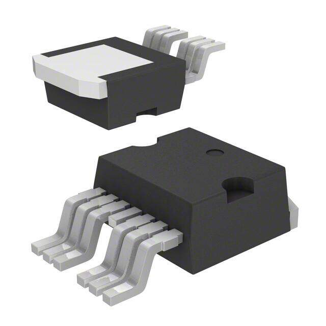
Package TO-263-7, D2Pak (6 Leads + Tab)
Category Discrete Semiconductor Products / Transistors - FETs, MOSFETs - Single
Description
MOSFET N-CH 75V 180A H2PAK-6
PDF
/
Buying Options
Total Price: USD $2.01
Unit Price: USD $2.01495
≥1 USD $2.01495
≥10 USD $1.653
≥100 USD $1.6017
≥500 USD $1.54945
≥1000 USD $1.49815
Inventory: 1245
Minimum: 1
-
+

Technical Details
Compliance
RoHS Status ROHS3 Compliant
Dimensions
Width 8.9mm
Length 10.4mm
Height 4.6mm
Technical
DS Breakdown Voltage-Min 75V
Pulsed Drain Current-Max (IDM) 720A
Drain-source On Resistance-Max 0.003Ohm
Gate to Source Voltage (Vgs) 20V
Continuous Drain Current (ID) 180A
Turn-Off Delay Time 100 ns
Vgs (Max) ±20V
Drive Voltage (Max Rds On,Min Rds On) 10V
Drain to Source Voltage (Vdss) 75V
Gate Charge (Qg) (Max) @ Vgs 87nC @ 10V
Current - Continuous Drain (Id) @ 25°C 180A Tc
Input Capacitance (Ciss) (Max) @ Vds 6800pF @ 25V
Vgs(th) (Max) @ Id 4V @ 250μA
Rds On (Max) @ Id, Vgs 3m Ω @ 90A, 10V
Transistor Application SWITCHING
FET Type N-Channel
Turn On Delay Time 25 ns
Case Connection DRAIN
Operating Mode ENHANCEMENT MODE
Element Configuration Single
Power Dissipation-Max 300W Tc
Number of Elements 1
Base Part Number STH245
Time@Peak Reflow Temperature-Max (s) NOT SPECIFIED
Peak Reflow Temperature (Cel) NOT SPECIFIED
Terminal Form GULL WING
Technology MOSFET (Metal Oxide)
ECCN Code EAR99
Number of Terminations 6
Moisture Sensitivity Level (MSL) 1 (Unlimited)
Part Status Obsolete
Series Automotive, AEC-Q101, STripFET? F3
Packaging Cut Tape (CT)
Operating Temperature -55°C~175°C TJ
Physical
Transistor Element Material SILICON
Number of Pins 6
Package / Case TO-263-7, D2Pak (6 Leads + Tab)
Mounting Type Surface Mount
Mount Surface Mount
Alternative Model

Recommended For You

STH245N75F3-6+price,STH245N75F3-6+datasheet,STH245N75F3-6+in stock,buy+STH245N75F3-6,finder+STH245N75F3-6,STH245N75F3-6+tutorials,STH245N75F3-6+download