STD8NF25
RoHS  RoHS compliant
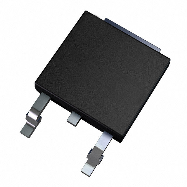
Package TO-252-3, DPak (2 Leads + Tab), SC-63
Category Discrete Semiconductor Products / Transistors - FETs, MOSFETs - Single
Description
Trans MOSFET N-CH 250V 8A Automotive 3-Pin(2+Tab) DPAK T/R
PDF
/
Buying Options
Total Price: USD $0.77
Unit Price: USD $0.7656
≥1 USD $0.7656
≥10 USD $0.66176
≥100 USD $0.458128
≥500 USD $0.382818
≥1000 USD $0.325802
Inventory: 1494
Minimum: 1
-
+

Technical Details
Compliance
Lead Free Lead Free
RoHS Status ROHS3 Compliant
Radiation Hardening No
Technical
Drain to Source Breakdown Voltage 250V
Drain Current-Max (Abs) (ID) 8A
Gate to Source Voltage (Vgs) 20V
Continuous Drain Current (ID) 8A
Turn-Off Delay Time 26 ns
Fall Time (Typ) 6 ns
Vgs (Max) ±20V
Drive Voltage (Max Rds On,Min Rds On) 10V
Rise Time 10 ns
Gate Charge (Qg) (Max) @ Vgs 16nC @ 10V
Current - Continuous Drain (Id) @ 25°C 8A Tc
Input Capacitance (Ciss) (Max) @ Vds 500pF @ 25V
Vgs(th) (Max) @ Id 4V @ 250μA
Rds On (Max) @ Id, Vgs 420m Ω @ 8A, 10V
Transistor Application SWITCHING
FET Type N-Channel
Turn On Delay Time 13 ns
Case Connection DRAIN
Power Dissipation 72W
Operating Mode ENHANCEMENT MODE
Power Dissipation-Max 72W Tc
Configuration SINGLE WITH BUILT-IN DIODE
Number of Elements 1
JESD-30 Code R-PSSO-G2
Base Part Number STD8N
Terminal Form GULL WING
Terminal Position SINGLE
Technology MOSFET (Metal Oxide)
Subcategory FET General Purpose Power
Terminal Finish Matte Tin (Sn) - annealed
Resistance 420MOhm
ECCN Code EAR99
Number of Terminations 2
Moisture Sensitivity Level (MSL) 1 (Unlimited)
Part Status Active
JESD-609 Code e3
Series STripFET? II
Packaging Tape & Reel (TR)
Operating Temperature -55°C~175°C TJ
Physical
Transistor Element Material SILICON
Number of Pins 3
Package / Case TO-252-3, DPak (2 Leads + Tab), SC-63
Mounting Type Surface Mount
Mount Surface Mount
Supply Chain
Lifecycle Status ACTIVE (Last Updated: 8 months ago)
Factory Lead Time 12 Weeks
Alternative Model

Recommended For You

STD8NF25+price,STD8NF25+datasheet,STD8NF25+in stock,buy+STD8NF25,finder+STD8NF25,STD8NF25+tutorials,STD8NF25+download