STB9NK70ZT4
RoHS  RoHS compliant
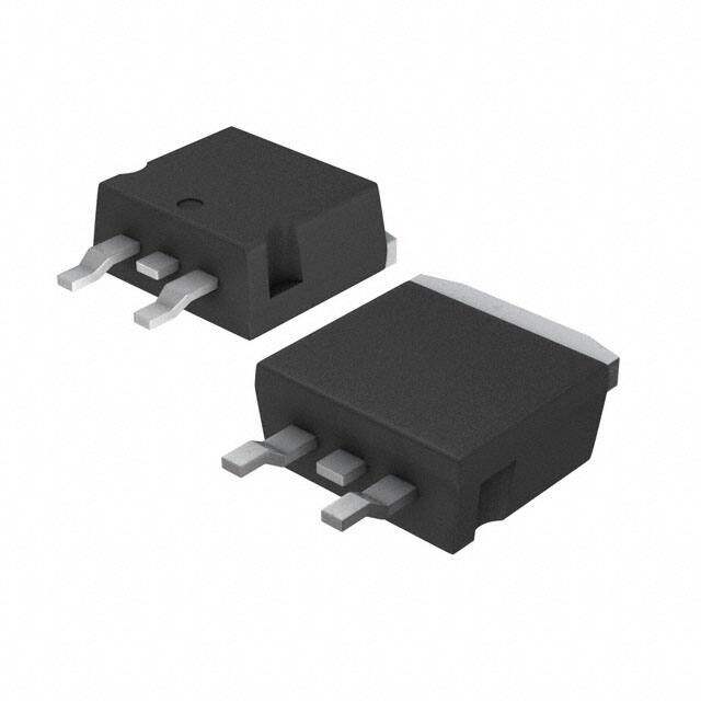
Package TO-263-3, D2Pak (2 Leads + Tab), TO-263AB
Category Discrete Semiconductor Products / Transistors - FETs, MOSFETs - Single
Description
MOSFET N-CH 700V 7.5A D2PAK
PDF
/
Buying Options
Total Price: USD $0.81
Unit Price: USD $0.8056
≥1 USD $0.8056
≥10 USD $0.6612
≥100 USD $0.6403
≥500 USD $0.62035
≥1000 USD $0.59945
Inventory: 3852
Minimum: 1
-
+

Technical Details
Technical
Rise Time 17 ns
Drive Voltage (Max Rds On,Min Rds On) 10V
Vgs (Max) ±30V
Fall Time (Typ) 13 ns
Turn-Off Delay Time 45 ns
Continuous Drain Current (ID) 7.5A
Gate to Source Voltage (Vgs) 30V
Drain to Source Breakdown Voltage 700V
Gate Charge (Qg) (Max) @ Vgs 68nC @ 10V
Current - Continuous Drain (Id) @ 25°C 7.5A Tc
Input Capacitance (Ciss) (Max) @ Vds 1370pF @ 25V
Vgs(th) (Max) @ Id 4.5V @ 100μA
Rds On (Max) @ Id, Vgs 1.2 Ω @ 4A, 10V
Transistor Application SWITCHING
FET Type N-Channel
Power Dissipation 115W
Operating Mode ENHANCEMENT MODE
Element Configuration Single
Power Dissipation-Max 115W Tc
Number of Elements 1
Qualification Status Not Qualified
JESD-30 Code R-PSSO-G2
Pin Count 3
Base Part Number STB9N
Time@Peak Reflow Temperature-Max (s) 30
Current Rating 7.5A
Reach Compliance Code not_compliant
Peak Reflow Temperature (Cel) 245
Terminal Form GULL WING
Technology MOSFET (Metal Oxide)
Voltage - Rated DC 700V
Subcategory FET General Purpose Power
Terminal Finish Matte Tin (Sn)
ECCN Code EAR99
Number of Terminations 2
Moisture Sensitivity Level (MSL) 1 (Unlimited)
Part Status Obsolete
JESD-609 Code e3
Series SuperMESH?
Packaging Tape & Reel (TR)
Operating Temperature -55°C~150°C TJ
Compliance
RoHS Status ROHS3 Compliant
Lead Free Lead Free
Physical
Transistor Element Material SILICON
Number of Pins 3
Package / Case TO-263-3, D2Pak (2 Leads + Tab), TO-263AB
Mounting Type Surface Mount
Mount Surface Mount
Alternative Model

Recommended For You

STB9NK70ZT4+price,STB9NK70ZT4+datasheet,STB9NK70ZT4+in stock,buy+STB9NK70ZT4,finder+STB9NK70ZT4,STB9NK70ZT4+tutorials,STB9NK70ZT4+download