STB11NK50ZT4
RoHS  RoHS compliant
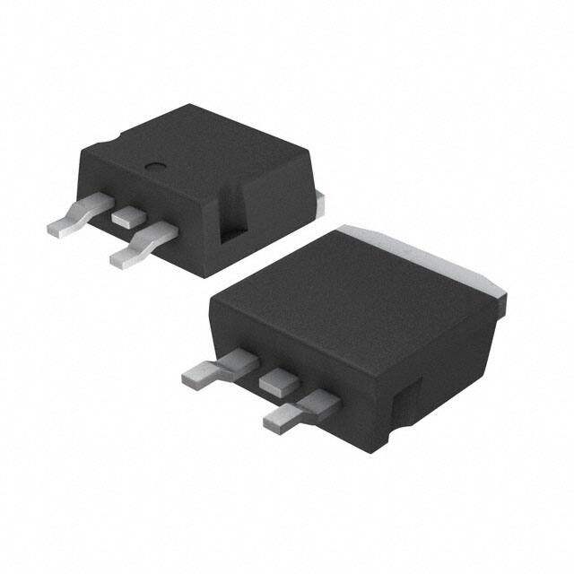
Package TO-263-3, D2Pak (2 Leads + Tab), TO-263AB
Category Discrete Semiconductor Products / Transistors - FETs, MOSFETs - Single
Description
MOSFET N-CH 500V 10A D2PAK
PDF
/
Buying Options
Total Price: USD $2.73
Unit Price: USD $2.728
≥1 USD $2.728
≥10 USD $2.288
≥100 USD $1.850728
≥500 USD $1.645054
Inventory: 944
Minimum: 1
-
+

Technical Details
Compliance
Lead Free Lead Free
RoHS Status ROHS3 Compliant
REACH SVHC No SVHC
Radiation Hardening No
Technical
Nominal Vgs 3.75 V
Dual Supply Voltage 500V
Pulsed Drain Current-Max (IDM) 40A
Drain to Source Breakdown Voltage 500V
Gate to Source Voltage (Vgs) 30V
Threshold Voltage 3.75V
Continuous Drain Current (ID) 4.5A
Turn-Off Delay Time 41 ns
Fall Time (Typ) 15 ns
Vgs (Max) ±30V
Drive Voltage (Max Rds On,Min Rds On) 10V
Rise Time 18 ns
Gate Charge (Qg) (Max) @ Vgs 68nC @ 10V
Current - Continuous Drain (Id) @ 25°C 10A Tc
Input Capacitance (Ciss) (Max) @ Vds 1390pF @ 25V
Vgs(th) (Max) @ Id 4.5V @ 100μA
Rds On (Max) @ Id, Vgs 520m Ω @ 4.5A, 10V
Transistor Application SWITCHING
FET Type N-Channel
Turn On Delay Time 14.5 ns
Power Dissipation 125W
Operating Mode ENHANCEMENT MODE
Element Configuration Single
Power Dissipation-Max 125W Tc
Number of Elements 1
JESD-30 Code R-PSSO-G2
Pin Count 3
Base Part Number STB11N
Time@Peak Reflow Temperature-Max (s) 30
Current Rating 10A
Peak Reflow Temperature (Cel) 245
Terminal Form GULL WING
Technology MOSFET (Metal Oxide)
Voltage - Rated DC 500V
Subcategory FET General Purpose Power
Additional Feature AVALANCHE RATED
Terminal Finish Matte Tin (Sn) - annealed
Resistance 520mOhm
ECCN Code EAR99
Termination SMD/SMT
Number of Terminations 2
Moisture Sensitivity Level (MSL) 1 (Unlimited)
Part Status Active
JESD-609 Code e3
Series SuperMESH?
Packaging Tape & Reel (TR)
Operating Temperature -55°C~150°C TJ
Physical
Transistor Element Material SILICON
Number of Pins 3
Package / Case TO-263-3, D2Pak (2 Leads + Tab), TO-263AB
Mounting Type Surface Mount
Mount Surface Mount
Supply Chain
Factory Lead Time 12 Weeks
Alternative Model

Recommended For You

STB11NK50ZT4+price,STB11NK50ZT4+datasheet,STB11NK50ZT4+in stock,buy+STB11NK50ZT4,finder+STB11NK50ZT4,STB11NK50ZT4+tutorials,STB11NK50ZT4+download