STB100NF03L-03-1
RoHS  RoHS compliant
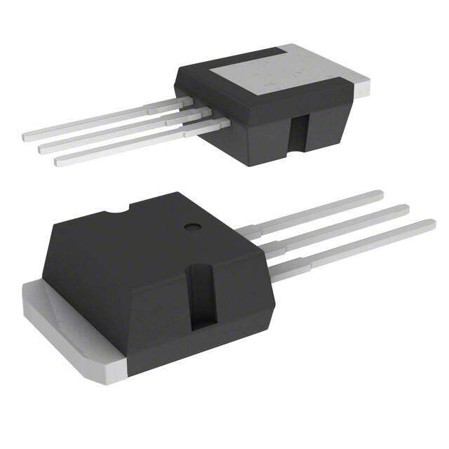
Package TO-262-3 Long Leads, I2Pak, TO-262AA
Category Discrete Semiconductor Products / Transistors - FETs, MOSFETs - Single
Description
MOSFET N-Ch 30 Volt 100 Amp
PDF
/
Buying Options
Total Price: USD $20.22
Unit Price: USD $20.22265
≥1 USD $20.22265
≥10 USD $16.5927
≥100 USD $16.074
≥500 USD $15.5553
≥1000 USD $15.03755
Inventory: 1144
Minimum: 1
-
+

Technical Details
Compliance
RoHS Status ROHS3 Compliant
Technical
Pulsed Drain Current-Max (IDM) 400A
Drain to Source Breakdown Voltage 30V
Drain-source On Resistance-Max 0.0045Ohm
Gate to Source Voltage (Vgs) 16V
Continuous Drain Current (ID) 100A
Turn-Off Delay Time 115 ns
Fall Time (Typ) 95 ns
Vgs (Max) ±16V
Drive Voltage (Max Rds On,Min Rds On) 4.5V 10V
Rise Time 315 ns
Gate Charge (Qg) (Max) @ Vgs 88nC @ 5V
Current - Continuous Drain (Id) @ 25°C 100A Tc
Input Capacitance (Ciss) (Max) @ Vds 6200pF @ 25V
Vgs(th) (Max) @ Id 2.5V @ 250μA
Rds On (Max) @ Id, Vgs 3.2m Ω @ 50A, 10V
Transistor Application SWITCHING
FET Type N-Channel
Turn On Delay Time 35 ns
Case Connection DRAIN
Power Dissipation 300W
Operating Mode ENHANCEMENT MODE
Element Configuration Single
Power Dissipation-Max 300W Tc
Number of Elements 1
Qualification Status Not Qualified
Pin Count 3
Base Part Number STB100N
Time@Peak Reflow Temperature-Max (s) NOT SPECIFIED
Reach Compliance Code not_compliant
Peak Reflow Temperature (Cel) NOT SPECIFIED
Technology MOSFET (Metal Oxide)
Subcategory FET General Purpose Power
Additional Feature LOGIC LEVEL COMPATIBLE
Terminal Finish Matte Tin (Sn)
ECCN Code EAR99
Number of Terminations 3
Moisture Sensitivity Level (MSL) 1 (Unlimited)
Part Status Obsolete
JESD-609 Code e3
Series STripFET? III
Packaging Tube
Operating Temperature -55°C~175°C TJ
Physical
Transistor Element Material SILICON
Number of Pins 3
Package / Case TO-262-3 Long Leads, I2Pak, TO-262AA
Mounting Type Through Hole
Mount Through Hole
Alternative Model

Recommended For You

STB100NF03L-03-1+price,STB100NF03L-03-1+datasheet,STB100NF03L-03-1+in stock,buy+STB100NF03L-03-1,finder+STB100NF03L-03-1,STB100NF03L-03-1+tutorials,STB100NF03L-03-1+download