2N7000
RoHS  RoHS compliant
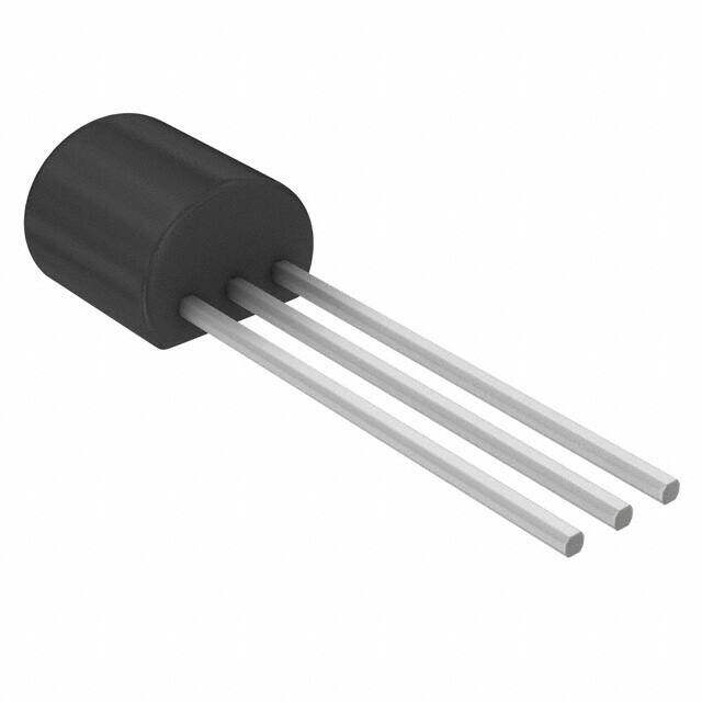
Package TO-226-3, TO-92-3 (TO-226AA)
Category Discrete Semiconductor Products / Transistors - FETs, MOSFETs - Single
Description
STripFET? Bulk Through Hole N-Channel Mosfet Transistor 350mA Tc 350mA 1W 8ns
PDF
/
Buying Options
Total Price: USD $0.35
Unit Price: USD $0.352
≥1 USD $0.352
≥10 USD $0.3344
≥100 USD $0.3168
≥500 USD $0.2992
≥1000 USD $0.29216
Inventory: 7675
Minimum: 1
-
+

Technical Details
Compliance
Lead Free Lead Free
RoHS Status ROHS3 Compliant
REACH SVHC No SVHC
Dimensions
Width 3.94mm
Length 4.95mm
Height 4.95mm
Technical
Nominal Vgs 2.1 V
Dual Supply Voltage 60V
Drain to Source Breakdown Voltage 60V
Gate to Source Voltage (Vgs) 18V
Threshold Voltage 2.1V
Continuous Drain Current (ID) 350mA
Turn-Off Delay Time 7 ns
Fall Time (Typ) 8 ns
Vgs (Max) ±18V
Drive Voltage (Max Rds On,Min Rds On) 4.5V 10V
Rise Time 15ns
Gate Charge (Qg) (Max) @ Vgs 2nC @ 5V
Current - Continuous Drain (Id) @ 25°C 350mA Tc
Input Capacitance (Ciss) (Max) @ Vds 43pF @ 25V
Vgs(th) (Max) @ Id 3V @ 250μA
Rds On (Max) @ Id, Vgs 5 Ω @ 500mA, 10V
Transistor Application SWITCHING
FET Type N-Channel
Turn On Delay Time 5 ns
Power Dissipation 1W
Operating Mode ENHANCEMENT MODE
Element Configuration Single
Power Dissipation-Max 1W Tc
Number of Elements 1
Lead Pitch 1.27mm
Qualification Status Not Qualified
Pin Count 3
Base Part Number 2N70
Time@Peak Reflow Temperature-Max (s) NOT SPECIFIED
Current Rating 200mA
Reach Compliance Code unknown
Peak Reflow Temperature (Cel) NOT SPECIFIED
Terminal Position BOTTOM
Technology MOSFET (Metal Oxide)
Voltage - Rated DC 60V
Subcategory FET General Purpose Power
Additional Feature LOW THRESHOLD
Resistance 5.3Ohm
ECCN Code EAR99
Number of Terminations 3
Moisture Sensitivity Level (MSL) 1 (Unlimited)
Part Status Obsolete
Pbfree Code yes
JESD-609 Code e3
Series STripFET?
Packaging Bulk
Operating Temperature -55°C~150°C TJ
Physical
Transistor Element Material SILICON
Number of Pins 3
Package / Case TO-226-3, TO-92-3 (TO-226AA)
Mounting Type Through Hole
Mount Through Hole
Contact Plating Tin
Recommended For You

2N7000+price,2N7000+datasheet,2N7000+in stock,buy+2N7000,finder+2N7000,2N7000+tutorials,2N7000+download