US5U35TR
RoHS  RoHS compliant
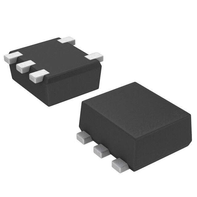
Package 6-SMD (5 Leads), Flat Lead
Category Discrete Semiconductor Products / Transistors - FETs, MOSFETs - Single
Description
MOSFET P-CH 45V 700MA TUMT5
PDF
/
Buying Options
Total Price: USD $0.63
Unit Price: USD $0.6336
≥1 USD $0.6336
≥10 USD $0.54912
≥100 USD $0.379984
≥500 USD $0.317486
≥1000 USD $0.270195
Inventory: 1116
Minimum: 1
-
+

Technical Details
Compliance
RoHS Status ROHS3 Compliant
Lead Free Lead Free
Radiation Hardening No
Technical
FET Feature Schottky Diode (Isolated)
Drain to Source Breakdown Voltage 25V
Drain Current-Max (Abs) (ID) 0.7A
Gate to Source Voltage (Vgs) 20V
Continuous Drain Current (ID) 700mA
Turn-Off Delay Time 17 ns
Fall Time (Typ) 5 ns
Vgs (Max) ±20V
Drive Voltage (Max Rds On,Min Rds On) 4V 10V
Drain to Source Voltage (Vdss) 45V
Rise Time 5ns
Gate Charge (Qg) (Max) @ Vgs 1.7nC @ 5V
Current - Continuous Drain (Id) @ 25°C 700mA Ta
Input Capacitance (Ciss) (Max) @ Vds 120pF @ 10V
Vgs(th) (Max) @ Id 2.5V @ 1mA
Rds On (Max) @ Id, Vgs 800m Ω @ 700mA, 10V
Transistor Application SWITCHING
FET Type P-Channel
Turn On Delay Time 6 ns
Power Dissipation 700mW
Operating Mode ENHANCEMENT MODE
Element Configuration Single
Power Dissipation-Max 1W Ta
Number of Elements 1
Pin Count 5
Time@Peak Reflow Temperature-Max (s) 10
Peak Reflow Temperature (Cel) 260
Terminal Position DUAL
Technology MOSFET (Metal Oxide)
Subcategory Other Transistors
Terminal Finish Tin/Copper (Sn/Cu)
Resistance 1.4Ohm
ECCN Code EAR99
Number of Terminations 5
Moisture Sensitivity Level (MSL) 1 (Unlimited)
Part Status Active
Pbfree Code yes
JESD-609 Code e2
Published 2008
Packaging Tape & Reel (TR)
Operating Temperature 150°C TJ
Physical
Transistor Element Material SILICON
Number of Pins 5
Package / Case 6-SMD (5 Leads), Flat Lead
Mounting Type Surface Mount
Mount Surface Mount
Supply Chain
Factory Lead Time 16 Weeks
Alternative Model

Recommended For You

US5U35TR+price,US5U35TR+datasheet,US5U35TR+in stock,buy+US5U35TR,finder+US5U35TR,US5U35TR+tutorials,US5U35TR+download