US5U1TR
RoHS  RoHS compliant
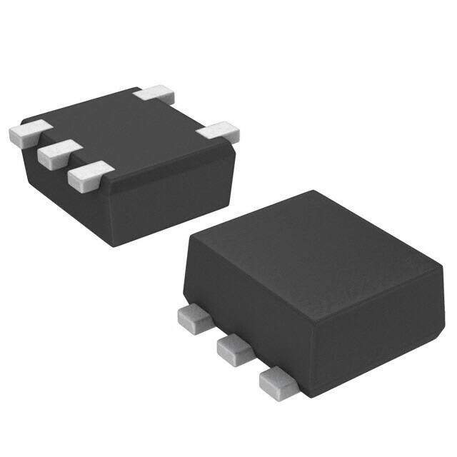
Package 6-SMD (5 Leads), Flat Lead
Category Discrete Semiconductor Products / Transistors - FETs, MOSFETs - Single
Description
MOSFET N-CH 30V 1.5A TUMT5
PDF
/
Buying Options
Total Price: USD $0.55
Unit Price: USD $0.5456
≥1 USD $0.5456
≥10 USD $0.47696
≥100 USD $0.33
≥500 USD $0.275704
≥1000 USD $0.234643
Inventory: 1096
Minimum: 1
-
+

Technical Details
Compliance
Lead Free Lead Free
RoHS Status ROHS3 Compliant
Radiation Hardening No
Dimensions
Width 1.6mm
Length 2.9mm
Height 850μm
Technical
FET Feature Schottky Diode (Isolated)
Drain to Source Breakdown Voltage 30V
Drain-source On Resistance-Max 0.34Ohm
Gate to Source Voltage (Vgs) 12V
Continuous Drain Current (ID) 1.5A
Turn-Off Delay Time 15 ns
Fall Time (Typ) 9 ns
Vgs (Max) ±12V
Drive Voltage (Max Rds On,Min Rds On) 2.5V 4.5V
Rise Time 9ns
Gate Charge (Qg) (Max) @ Vgs 2.2nC @ 4.5V
Current - Continuous Drain (Id) @ 25°C 1.5A Ta
Input Capacitance (Ciss) (Max) @ Vds 80pF @ 10V
Vgs(th) (Max) @ Id 1.5V @ 1mA
Rds On (Max) @ Id, Vgs 240m Ω @ 1.5A, 4.5V
Transistor Application SWITCHING
FET Type N-Channel
Turn On Delay Time 7 ns
Power Dissipation 700mW
Operating Mode ENHANCEMENT MODE
Element Configuration Single
Power Dissipation-Max 1W Ta
Number of Elements 1
Pin Count 5
Time@Peak Reflow Temperature-Max (s) 10
Current Rating 1.5A
Peak Reflow Temperature (Cel) 260
Terminal Position DUAL
Technology MOSFET (Metal Oxide)
Voltage - Rated DC 30V
Subcategory FET General Purpose Powers
Terminal Finish TIN COPPER
ECCN Code EAR99
Number of Terminations 5
Moisture Sensitivity Level (MSL) 1 (Unlimited)
Part Status Active
Pbfree Code yes
JESD-609 Code e2
Published 2007
Packaging Tape & Reel (TR)
Operating Temperature 150°C TJ
Physical
Transistor Element Material SILICON
Number of Pins 5
Package / Case 6-SMD (5 Leads), Flat Lead
Mounting Type Surface Mount
Mount Surface Mount
Supply Chain
Factory Lead Time 16 Weeks
Alternative Model

Recommended For You

US5U1TR+price,US5U1TR+datasheet,US5U1TR+in stock,buy+US5U1TR,finder+US5U1TR,US5U1TR+tutorials,US5U1TR+download