RUR040N02TL
RoHS  RoHS compliant
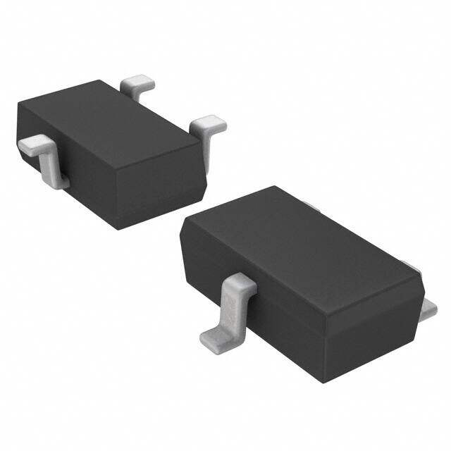
Package SC-96
Category Discrete Semiconductor Products / Transistors - FETs, MOSFETs - Single
Description
MOSFET N-CH 20V 4A TSMT3
PDF
/
Buying Options
Total Price: USD $0.58
Unit Price: USD $0.5808
≥1 USD $0.5808
≥10 USD $0.49984
≥100 USD $0.345928
≥500 USD $0.28908
≥1000 USD $0.246022
Inventory: 1188
Minimum: 1
-
+

Technical Details
Compliance
RoHS Status ROHS3 Compliant
REACH SVHC No SVHC
Radiation Hardening No
Dimensions
Width 1.6mm
Length 2.9mm
Height 800μm
Technical
Nominal Vgs 300 mV
Drain to Source Breakdown Voltage 20V
Drain-source On Resistance-Max 0.046Ohm
Drain Current-Max (Abs) (ID) 4A
Gate to Source Voltage (Vgs) 10V
Continuous Drain Current (ID) 4A
Turn-Off Delay Time 50 ns
Fall Time (Typ) 60 ns
Vgs (Max) ±10V
Drive Voltage (Max Rds On,Min Rds On) 1.5V 4.5V
Rise Time 30 ns
Gate Charge (Qg) (Max) @ Vgs 8nC @ 4.5V
Current - Continuous Drain (Id) @ 25°C 4A Ta
Input Capacitance (Ciss) (Max) @ Vds 680pF @ 10V
Vgs(th) (Max) @ Id 1.3V @ 1mA
Rds On (Max) @ Id, Vgs 35m Ω @ 4A, 4.5V
Transistor Application SWITCHING
FET Type N-Channel
Turn On Delay Time 10 ns
Power Dissipation 1W
Operating Mode ENHANCEMENT MODE
Element Configuration Single
Power Dissipation-Max 1W Ta
Number of Elements 1
Pin Count 3
Time@Peak Reflow Temperature-Max (s) 10
Peak Reflow Temperature (Cel) 260
Terminal Form GULL WING
Terminal Position DUAL
Technology MOSFET (Metal Oxide)
Subcategory FET General Purpose Power
ECCN Code EAR99
Number of Terminations 3
Moisture Sensitivity Level (MSL) 1 (Unlimited)
Part Status Active
Pbfree Code yes
JESD-609 Code e1
Published 1999
Packaging Tape & Reel (TR)
Operating Temperature 150°C TJ
Physical
Transistor Element Material SILICON
Number of Pins 3
Package / Case SC-96
Mounting Type Surface Mount
Mount Surface Mount
Supply Chain
Factory Lead Time 20 Weeks
Alternative Model

Recommended For You

RUR040N02TL+price,RUR040N02TL+datasheet,RUR040N02TL+in stock,buy+RUR040N02TL,finder+RUR040N02TL,RUR040N02TL+tutorials,RUR040N02TL+download