RQ3E080GNTB
RoHS  RoHS compliant
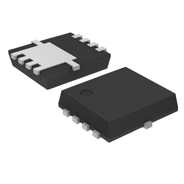
Package 8-PowerVDFN
Category Discrete Semiconductor Products / Transistors - FETs, MOSFETs - Single
Description
MOSFET N-CH 30V 8A 8-HSMT
PDF
/
Buying Options
Total Price: USD $0.45
Unit Price: USD $0.4488
≥1 USD $0.4488
≥10 USD $0.3476
≥100 USD $0.208736
≥500 USD $0.193318
≥1000 USD $0.131454
Inventory: 1096
Minimum: 1
-
+

Technical Details
Compliance
Lead Free Lead Free
RoHS Status ROHS3 Compliant
Dimensions
Height 900μm
Technical
Max Junction Temperature (Tj) 150°C
Pulsed Drain Current-Max (IDM) 32A
Drain to Source Breakdown Voltage 30V
Drain Current-Max (Abs) (ID) 8A
Gate to Source Voltage (Vgs) 20V
Continuous Drain Current (ID) 8A
Turn-Off Delay Time 17.3 ns
Fall Time (Typ) 2.4 ns
Vgs (Max) ±20V
Drive Voltage (Max Rds On,Min Rds On) 4.5V 10V
Rise Time 3.6 ns
Gate Charge (Qg) (Max) @ Vgs 5.8nC @ 10V
Current - Continuous Drain (Id) @ 25°C 8A Ta
Input Capacitance (Ciss) (Max) @ Vds 295pF @ 15V
Vgs(th) (Max) @ Id 2.5V @ 1mA
Rds On (Max) @ Id, Vgs 16.7m Ω @ 8A, 10V
Transistor Application SWITCHING
FET Type N-Channel
Turn On Delay Time 6.9 ns
Case Connection DRAIN
Power Dissipation 2W
Operating Mode ENHANCEMENT MODE
Element Configuration Single
Power Dissipation-Max 2W Ta 15W Tc
Number of Channels 1
Number of Elements 1
JESD-30 Code R-PDSO-F5
Time@Peak Reflow Temperature-Max (s) NOT SPECIFIED
Reach Compliance Code not_compliant
Peak Reflow Temperature (Cel) NOT SPECIFIED
Terminal Form FLAT
Terminal Position DUAL
Technology MOSFET (Metal Oxide)
ECCN Code EAR99
Number of Terminations 5
Moisture Sensitivity Level (MSL) 1 (Unlimited)
Part Status Active
Published 2013
Packaging Tape & Reel (TR)
Operating Temperature 150°C TJ
Physical
Transistor Element Material SILICON
Number of Pins 8
Package / Case 8-PowerVDFN
Mounting Type Surface Mount
Mount Surface Mount
Supply Chain
Factory Lead Time 20 Weeks
Alternative Model

Recommended For You

RQ3E080GNTB+price,RQ3E080GNTB+datasheet,RQ3E080GNTB+in stock,buy+RQ3E080GNTB,finder+RQ3E080GNTB,RQ3E080GNTB+tutorials,RQ3E080GNTB+download