R5205CNDTL
RoHS  RoHS compliant
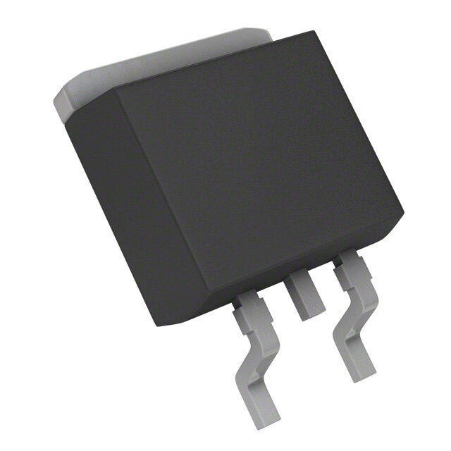
Package TO-252-3, DPak (2 Leads + Tab), SC-63
Category Discrete Semiconductor Products / Transistors - FETs, MOSFETs - Single
Description
MOSFET N-CH 10V DRIVE CPT
PDF
/
Buying Options
Total Price: USD $3.05
Unit Price: USD $3.048439
≥1 USD $3.048439
≥10 USD $2.875881
≥100 USD $2.713103
≥500 USD $2.559522
≥1000 USD $2.414651
Inventory: 1178
Minimum: 1
-
+

Technical Details
Compliance
Lead Free Lead Free
RoHS Status ROHS3 Compliant
Radiation Hardening No
Technical
DS Breakdown Voltage-Min 525V
Pulsed Drain Current-Max (IDM) 20A
Drain Current-Max (Abs) (ID) 5A
Gate to Source Voltage (Vgs) 30V
Continuous Drain Current (ID) 5A
Turn-Off Delay Time 40 ns
Fall Time (Typ) 20 ns
Vgs (Max) ±30V
Drive Voltage (Max Rds On,Min Rds On) 10V
Drain to Source Voltage (Vdss) 525V
Rise Time 25ns
Gate Charge (Qg) (Max) @ Vgs 10.8nC @ 10V
Current - Continuous Drain (Id) @ 25°C 5A Ta
Input Capacitance (Ciss) (Max) @ Vds 320pF @ 25V
Vgs(th) (Max) @ Id 4.5V @ 1mA
Rds On (Max) @ Id, Vgs 1.6 Ω @ 2.5A, 10V
Transistor Application SWITCHING
FET Type N-Channel
Turn On Delay Time 20 ns
Operating Mode ENHANCEMENT MODE
Power Dissipation-Max 40W Tc
Number of Channels 1
Configuration SINGLE WITH BUILT-IN DIODE
Number of Elements 1
JESD-30 Code R-PSSO-G2
Pin Count 3
Time@Peak Reflow Temperature-Max (s) 10
Peak Reflow Temperature (Cel) 260
Terminal Form GULL WING
Terminal Position SINGLE
Technology MOSFET (Metal Oxide)
Subcategory FET General Purpose Power
Terminal Finish Tin/Copper (Sn98Cu2)
Number of Terminations 2
Moisture Sensitivity Level (MSL) 1 (Unlimited)
Part Status Not For New Designs
Pbfree Code yes
JESD-609 Code e2
Published 2010
Packaging Tape & Reel (TR)
Operating Temperature 150°C TJ
Physical
Transistor Element Material SILICON
Number of Pins 3
Package / Case TO-252-3, DPak (2 Leads + Tab), SC-63
Mounting Type Surface Mount
Mount Surface Mount
Supply Chain
Factory Lead Time 17 Weeks
Alternative Model

Recommended For You

R5205CNDTL+price,R5205CNDTL+datasheet,R5205CNDTL+in stock,buy+R5205CNDTL,finder+R5205CNDTL,R5205CNDTL+tutorials,R5205CNDTL+download