R5013ANJTL
RoHS  RoHS compliant
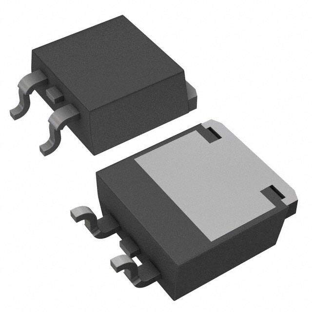
Package TO-263-3, D2Pak (2 Leads + Tab), TO-263AB
Category Discrete Semiconductor Products / Transistors - FETs, MOSFETs - Single
Description
MOSFET N-CH 10V DRIVE LPTS
PDF
/
Buying Options
Total Price: USD $4.98
Unit Price: USD $4.9803
≥1 USD $4.9803
≥10 USD $4.698405
≥100 USD $4.432458
≥500 USD $4.181568
≥1000 USD $3.944869
Inventory: 1195
Minimum: 1
-
+

Technical Details
Compliance
Lead Free Lead Free
RoHS Status ROHS3 Compliant
Radiation Hardening No
Technical
DS Breakdown Voltage-Min 500V
Pulsed Drain Current-Max (IDM) 52A
Gate to Source Voltage (Vgs) 30V
Continuous Drain Current (ID) 13A
Turn-Off Delay Time 90 ns
Fall Time (Typ) 30 ns
Vgs (Max) ±30V
Drive Voltage (Max Rds On,Min Rds On) 10V
Drain to Source Voltage (Vdss) 500V
Rise Time 32ns
Gate Charge (Qg) (Max) @ Vgs 35nC @ 10V
Current - Continuous Drain (Id) @ 25°C 13A Ta
Input Capacitance (Ciss) (Max) @ Vds 1300pF @ 25V
Vgs(th) (Max) @ Id 4.5V @ 1mA
Rds On (Max) @ Id, Vgs 380m Ω @ 6.5A, 10V
Transistor Application SWITCHING
FET Type N-Channel
Turn On Delay Time 30 ns
Operating Mode ENHANCEMENT MODE
Power Dissipation-Max 100W Tc
Number of Channels 1
Configuration SINGLE WITH BUILT-IN DIODE
Number of Elements 1
JESD-30 Code R-PSSO-G2
Pin Count 3
Time@Peak Reflow Temperature-Max (s) 10
Peak Reflow Temperature (Cel) 260
Terminal Form GULL WING
Terminal Position SINGLE
Technology MOSFET (Metal Oxide)
Subcategory FET General Purpose Power
Terminal Finish Tin/Copper (Sn/Cu)
Number of Terminations 2
Moisture Sensitivity Level (MSL) 1 (Unlimited)
Part Status Not For New Designs
Pbfree Code yes
JESD-609 Code e2
Published 2009
Packaging Tape & Reel (TR)
Operating Temperature 150°C TJ
Physical
Transistor Element Material SILICON
Number of Pins 3
Package / Case TO-263-3, D2Pak (2 Leads + Tab), TO-263AB
Mounting Type Surface Mount
Mount Surface Mount
Alternative Model

Recommended For You

R5013ANJTL+price,R5013ANJTL+datasheet,R5013ANJTL+in stock,buy+R5013ANJTL,finder+R5013ANJTL,R5013ANJTL+tutorials,R5013ANJTL+download