2SK3018T106
RoHS  RoHS compliant
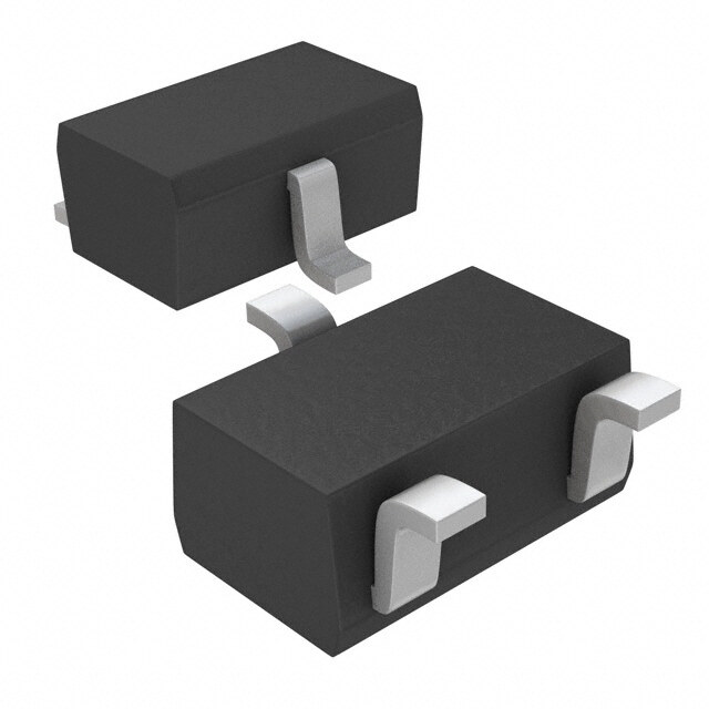
Package SC-70, SOT-323
Category Discrete Semiconductor Products / Transistors - FETs, MOSFETs - Single
Description
MOSFET N-CH 30V .1A SOT-323
PDF
/
Buying Options
Total Price: USD $0.04
Unit Price: USD $0.039105
≥1 USD $0.039105
≥10 USD $0.031982
≥100 USD $0.02842
≥500 USD $0.022259
≥1000 USD $0.020122
Inventory: 1232
Minimum: 1
-
+

Technical Details
Compliance
Lead Free Lead Free
RoHS Status ROHS3 Compliant
REACH SVHC No SVHC
Radiation Hardening No
Dimensions
Width 1.25mm
Length 2mm
Height 800μm
Technical
Nominal Vgs 1.5 V
Dual Supply Voltage 30V
Drain to Source Breakdown Voltage 30V
Drain Current-Max (Abs) (ID) 0.1A
Gate to Source Voltage (Vgs) 20V
Threshold Voltage 1.5V
Continuous Drain Current (ID) 100mA
Turn-Off Delay Time 80 ns
Fall Time (Typ) 35 ns
Vgs (Max) ±20V
Drive Voltage (Max Rds On,Min Rds On) 2.5V 4V
Rise Time 35ns
Current - Continuous Drain (Id) @ 25°C 100mA Ta
Input Capacitance (Ciss) (Max) @ Vds 13pF @ 5V
Vgs(th) (Max) @ Id 1.5V @ 100μA
Rds On (Max) @ Id, Vgs 8 Ω @ 10mA, 4V
Transistor Application SWITCHING
FET Type N-Channel
Turn On Delay Time 15 ns
Power Dissipation 200mW
Operating Mode ENHANCEMENT MODE
Element Configuration Single
Power Dissipation-Max 200mW Ta
Number of Elements 1
Pin Count 3
Time@Peak Reflow Temperature-Max (s) 10
Current Rating 100mA
Peak Reflow Temperature (Cel) 260
Terminal Form GULL WING
Terminal Position DUAL
Technology MOSFET (Metal Oxide)
Voltage - Rated DC 30V
Subcategory FET General Purpose Powers
Resistance 13Ohm
ECCN Code EAR99
Termination SMD/SMT
Number of Terminations 3
Moisture Sensitivity Level (MSL) 1 (Unlimited)
Part Status Not For New Designs
Pbfree Code yes
Published 2006
Packaging Tape & Reel (TR)
Operating Temperature 150°C TJ
Physical
Transistor Element Material SILICON
Number of Pins 3
Package / Case SC-70, SOT-323
Mounting Type Surface Mount
Mount Surface Mount
Contact Plating Copper, Silver, Tin
Supply Chain
Factory Lead Time 18 Weeks
Alternative Model

Recommended For You

2SK3018T106+price,2SK3018T106+datasheet,2SK3018T106+in stock,buy+2SK3018T106,finder+2SK3018T106,2SK3018T106+tutorials,2SK3018T106+download