2SK2463T100
RoHS  RoHS compliant
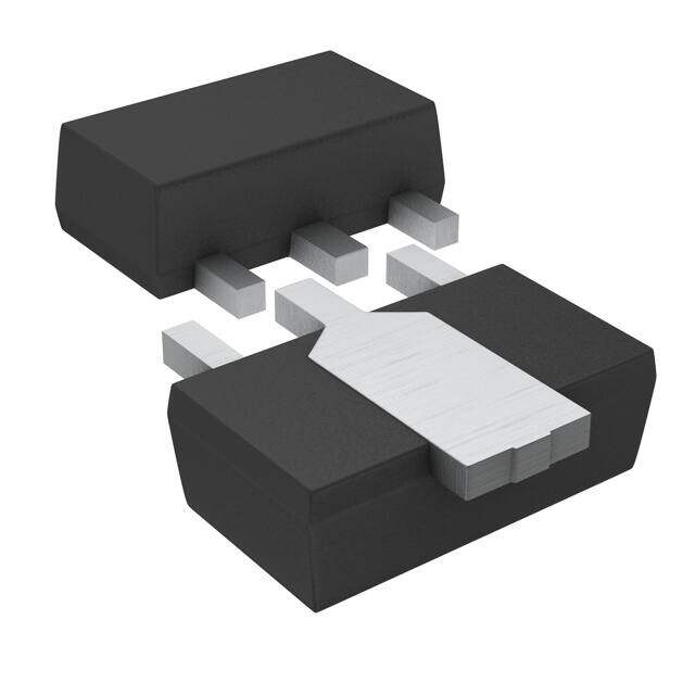
Package TO-243AA
Category Discrete Semiconductor Products / Transistors - FETs, MOSFETs - Single
Description
MOSFET N-CH 60V 2A MPT3
PDF
/
Buying Options
Total Price: USD $0.7
Unit Price: USD $0.6952
≥1 USD $0.6952
≥10 USD $0.60368
≥100 USD $0.418
≥500 USD $0.349219
Inventory: 917
Minimum: 1
-
+

Technical Details
Compliance
Lead Free Lead Free
RoHS Status ROHS3 Compliant
Technical
Drain to Source Breakdown Voltage 60V
Drain-source On Resistance-Max 0.58Ohm
Drain Current-Max (Abs) (ID) 2A
Gate to Source Voltage (Vgs) 20V
Continuous Drain Current (ID) 2A
Turn-Off Delay Time 50 ns
Fall Time (Typ) 50 ns
Vgs (Max) ±20V
Drive Voltage (Max Rds On,Min Rds On) 4V 10V
Rise Time 25ns
Current - Continuous Drain (Id) @ 25°C 2A Ta
Input Capacitance (Ciss) (Max) @ Vds 200pF @ 10V
Vgs(th) (Max) @ Id 2.5V @ 1mA
Rds On (Max) @ Id, Vgs 380m Ω @ 1A, 10V
Transistor Application SWITCHING
FET Type N-Channel
Case Connection DRAIN
Power Dissipation 500mW
Operating Mode ENHANCEMENT MODE
Element Configuration Single
Power Dissipation-Max 500mW Ta
Number of Elements 1
Qualification Status Not Qualified
Time@Peak Reflow Temperature-Max (s) 10
Reach Compliance Code not_compliant
Peak Reflow Temperature (Cel) 260
Terminal Form FLAT
Technology MOSFET (Metal Oxide)
HTS Code 8541.29.00.95
ECCN Code EAR99
Number of Terminations 3
Moisture Sensitivity Level (MSL) 1 (Unlimited)
Part Status Not For New Designs
Published 1998
Packaging Tape & Reel (TR)
Operating Temperature 150°C TJ
Physical
Transistor Element Material SILICON
Number of Pins 3
Package / Case TO-243AA
Mounting Type Surface Mount
Mount Surface Mount
Supply Chain
Factory Lead Time 7 Weeks
Alternative Model

Recommended For You

2SK2463T100+price,2SK2463T100+datasheet,2SK2463T100+in stock,buy+2SK2463T100,finder+2SK2463T100,2SK2463T100+tutorials,2SK2463T100+download