HAT2192WP-EL-E
RoHS  RoHS compliant
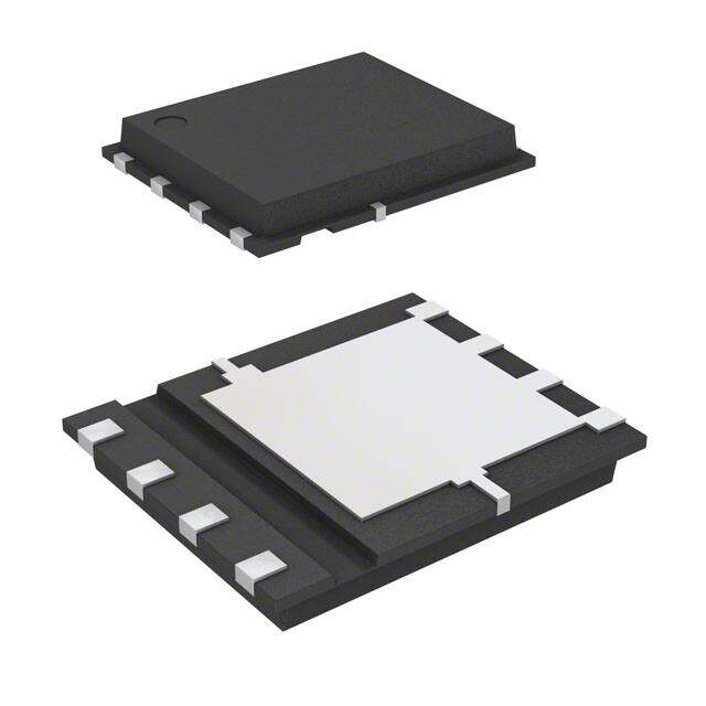
Package 8-PowerWDFN
Category Discrete Semiconductor Products / Transistors - FETs, MOSFETs - Single
Description
Trans MOSFET N-CH 250V 10A Automotive 8-Pin WPAK EP T/R
PDF
/
Buying Options
Total Price: USD $1.07
Unit Price: USD $1.07445
≥1 USD $1.07445
≥10 USD $0.8816
≥100 USD $0.85405
≥500 USD $0.8265
≥1000 USD $0.79895
Inventory: 1131
Minimum: 1
-
+

Technical Details
Compliance
RoHS Status ROHS3 Compliant
Technical
DS Breakdown Voltage-Min 250V
Pulsed Drain Current-Max (IDM) 20A
Drain-source On Resistance-Max 0.23Ohm
Gate to Source Voltage (Vgs) 30V
Continuous Drain Current (ID) 10A
Vgs (Max) ±30V
Drive Voltage (Max Rds On,Min Rds On) 10V
Drain to Source Voltage (Vdss) 250V
Gate Charge (Qg) (Max) @ Vgs 15nC @ 10V
Current - Continuous Drain (Id) @ 25°C 10A Ta
Input Capacitance (Ciss) (Max) @ Vds 710pF @ 25V
Rds On (Max) @ Id, Vgs 230m Ω @ 5A, 10V
Transistor Application SWITCHING
FET Type N-Channel
Case Connection DRAIN
Power Dissipation 25W
Operating Mode ENHANCEMENT MODE
Power Dissipation-Max 25W Tc
Configuration SINGLE WITH BUILT-IN DIODE
Number of Elements 1
Qualification Status Not Qualified
JESD-30 Code R-XDSO-N5
Pin Count 8
Time@Peak Reflow Temperature-Max (s) NOT SPECIFIED
Peak Reflow Temperature (Cel) 260
Terminal Form NO LEAD
Terminal Position DUAL
Technology MOSFET (Metal Oxide)
Subcategory FET General Purpose Power
ECCN Code EAR99
Number of Terminations 5
Moisture Sensitivity Level (MSL) 1 (Unlimited)
Part Status Active
Pbfree Code yes
Published 2001
Packaging Tape & Reel (TR)
Operating Temperature 150°C TJ
Physical
Transistor Element Material SILICON
Number of Pins 8
Package / Case 8-PowerWDFN
Mounting Type Surface Mount
Mount Surface Mount
Supply Chain
Factory Lead Time 16 Weeks
Alternative Model

Recommended For You

HAT2192WP-EL-E+price,HAT2192WP-EL-E+datasheet,HAT2192WP-EL-E+in stock,buy+HAT2192WP-EL-E,finder+HAT2192WP-EL-E,HAT2192WP-EL-E+tutorials,HAT2192WP-EL-E+download