MTM761230LBF
RoHS  RoHS compliant
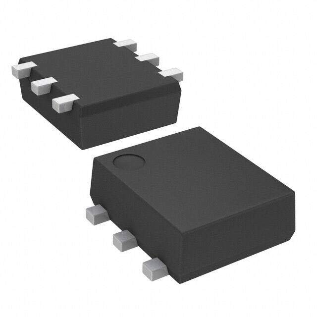
Package 6-SMD, Flat Leads
Category Discrete Semiconductor Products / Transistors - FETs, MOSFETs - Single
Description
MOSFET PCH MOS FET FLT LD 2.0x2.1mm
PDF
/
Buying Options
Total Price: USD $0.14
Unit Price: USD $0.1387
≥1 USD $0.1387
≥10 USD $0.114
≥100 USD $0.1102
≥500 USD $0.1064
≥1000 USD $0.10355
≥10000 USD $0.09215
Inventory: 74547
Minimum: 1
-
+

Technical Details
Compliance
Lead Free Lead Free
RoHS Status RoHS Compliant
REACH SVHC No SVHC
Dimensions
Width 1.7mm
Length 2mm
Height 700μm
Technical
Nominal Vgs 850 mV
Drain to Source Breakdown Voltage -20V
Drain Current-Max (Abs) (ID) 3A
Gate to Source Voltage (Vgs) 10V
Threshold Voltage -850mV
Continuous Drain Current (ID) -3A
Vgs (Max) ±10V
Drive Voltage (Max Rds On,Min Rds On) 2.5V 4V
Drain to Source Voltage (Vdss) 20V
Current - Continuous Drain (Id) @ 25°C 3A Ta
Input Capacitance (Ciss) (Max) @ Vds 1000pF @ 10V
Vgs(th) (Max) @ Id 1.3V @ 1mA
Rds On (Max) @ Id, Vgs 55m Ω @ 1A, 4V
Transistor Application SWITCHING
FET Type P-Channel
Power Dissipation 700mW
Operating Mode DEPLETION MODE
Element Configuration Single
Power Dissipation-Max 700mW Ta
Number of Elements 1
Time@Peak Reflow Temperature-Max (s) NOT SPECIFIED
Reach Compliance Code unknown
Peak Reflow Temperature (Cel) NOT SPECIFIED
Terminal Position DUAL
Technology MOSFET (Metal Oxide)
Subcategory Other Transistors
Resistance 55mOhm
ECCN Code EAR99
Number of Terminations 6
Moisture Sensitivity Level (MSL) 1 (Unlimited)
Part Status Active
Packaging Tape & Reel (TR)
Operating Temperature 150°C TJ
Physical
Transistor Element Material SILICON
Number of Pins 6
Package / Case 6-SMD, Flat Leads
Mounting Type Surface Mount
Mount Surface Mount
Supply Chain
Factory Lead Time 10 Weeks
Alternative Model

Recommended For You

MTM761230LBF+price,MTM761230LBF+datasheet,MTM761230LBF+in stock,buy+MTM761230LBF,finder+MTM761230LBF,MTM761230LBF+tutorials,MTM761230LBF+download