STD5407NT4G
RoHS
/
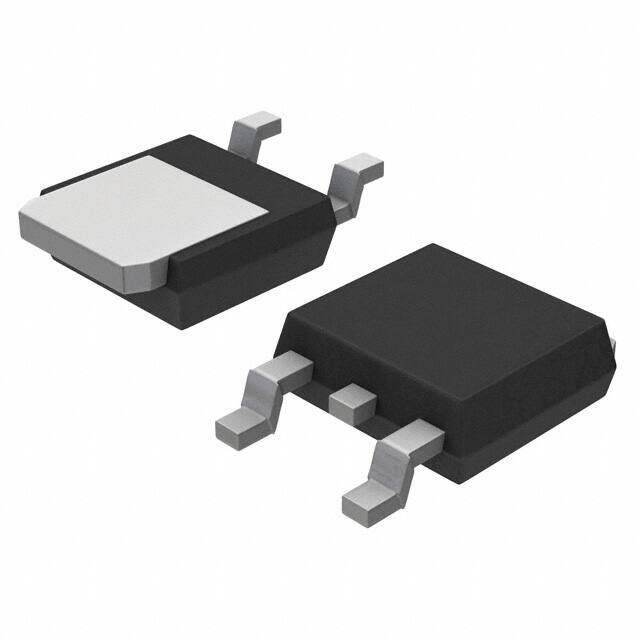
Package TO-252-3, DPak (2 Leads + Tab), SC-63
Category Discrete Semiconductor Products / Transistors - FETs, MOSFETs - Single
Description
MOSFET N-CH 40V 7.6A DPAK
PDF
/
Buying Options
Total Price: USD $0.24
Unit Price: USD $0.2376
≥1 USD $0.2376
Inventory: 134158
Minimum: 1
-
+

Technical Details
Compliance
Lead Free Lead Free
RoHS Status RoHS Compliant
Radiation Hardening No
Technical
DS Breakdown Voltage-Min 40V
Pulsed Drain Current-Max (IDM) 75A
Drain-source On Resistance-Max 0.026Ohm
Gate to Source Voltage (Vgs) 20V
Continuous Drain Current (ID) 7.6A
Vgs (Max) ±20V
Drive Voltage (Max Rds On,Min Rds On) 5V 10V
Drain to Source Voltage (Vdss) 40V
Gate Charge (Qg) (Max) @ Vgs 20nC @ 10V
Current - Continuous Drain (Id) @ 25°C 7.6A Ta 38A Tc
Input Capacitance (Ciss) (Max) @ Vds 1000pF @ 32V
Vgs(th) (Max) @ Id 3.5V @ 250μA
Rds On (Max) @ Id, Vgs 26m Ω @ 20A, 10V
Transistor Application SWITCHING
FET Type N-Channel
Case Connection DRAIN
Power Dissipation 2.9W
Operating Mode ENHANCEMENT MODE
Element Configuration Single
Power Dissipation-Max 2.9W Ta 75W Tc
Number of Elements 1
JESD-30 Code R-PSSO-G2
Pin Count 3
Terminal Form GULL WING
Technology MOSFET (Metal Oxide)
Subcategory FET General Purpose Power
Terminal Finish Tin (Sn)
ECCN Code EAR99
Number of Terminations 2
Moisture Sensitivity Level (MSL) 1 (Unlimited)
Part Status Obsolete
Pbfree Code yes
JESD-609 Code e3
Published 2013
Packaging Tape & Reel (TR)
Operating Temperature -55°C~175°C TJ
Physical
Transistor Element Material SILICON
Number of Pins 3
Surface Mount YES
Package / Case TO-252-3, DPak (2 Leads + Tab), SC-63
Mounting Type Surface Mount
Supply Chain
Lifecycle Status CONSULT SALES OFFICE (Last Updated: 1 week ago)
Factory Lead Time 24 Weeks
Alternative Model

Recommended For You

STD5407NT4G+price,STD5407NT4G+datasheet,STD5407NT4G+in stock,buy+STD5407NT4G,finder+STD5407NT4G,STD5407NT4G+tutorials,STD5407NT4G+download