SSN1N45BTA
RoHS  RoHS compliant
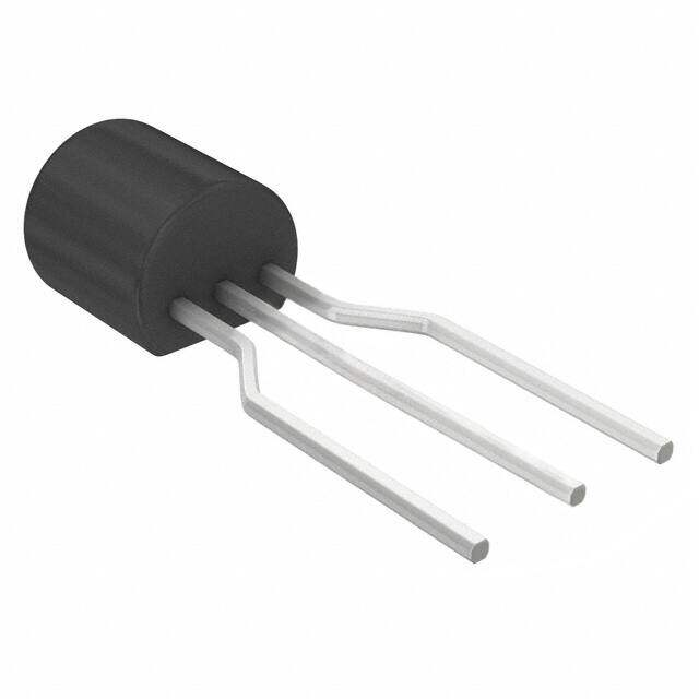
Package TO-226-3, TO-92-3 (TO-226AA) (Formed Leads)
Category Discrete Semiconductor Products / Transistors - FETs, MOSFETs - Single
Description
MOSFET N-CH 450V 500MA TO-92
PDF
/
Buying Options
Total Price: USD $0.8
Unit Price: USD $0.8008
≥1 USD $0.8008
≥10 USD $0.69344
≥100 USD $0.479952
≥500 USD $0.401034
≥1000 USD $0.341299
Inventory: 41366
Minimum: 1
-
+

Technical Details
Compliance
Lead Free Lead Free
RoHS Status ROHS3 Compliant
REACH SVHC No SVHC
Radiation Hardening No
Technical
Feedback Cap-Max (Crss) 8.5 pF
Drain to Source Breakdown Voltage 450V
Drain Current-Max (Abs) (ID) 0.5A
Gate to Source Voltage (Vgs) 50V
Continuous Drain Current (ID) 500mA
Turn-Off Delay Time 23 ns
Fall Time (Typ) 21 ns
Vgs (Max) ±50V
Drive Voltage (Max Rds On,Min Rds On) 10V
Rise Time 21 ns
Gate Charge (Qg) (Max) @ Vgs 8.5nC @ 10V
Current - Continuous Drain (Id) @ 25°C 500mA Tc
Input Capacitance (Ciss) (Max) @ Vds 240pF @ 25V
Vgs(th) (Max) @ Id 3.7V @ 250μA
Rds On (Max) @ Id, Vgs 4.25 Ω @ 250mA, 10V
Transistor Application SWITCHING
FET Type N-Channel
Turn On Delay Time 7.5 ns
Power Dissipation 900mW
Operating Mode ENHANCEMENT MODE
Element Configuration Single
Power Dissipation-Max 900mW Ta
Number of Elements 1
Current Rating 500mA
Terminal Position BOTTOM
Technology MOSFET (Metal Oxide)
Voltage - Rated DC 450V
Subcategory FET General Purpose Power
Terminal Finish Tin (Sn)
ECCN Code EAR99
Number of Terminations 3
Moisture Sensitivity Level (MSL) 1 (Unlimited)
Part Status Active
Pbfree Code yes
JESD-609 Code e3
Packaging Tape & Box (TB)
Operating Temperature -55°C~150°C TJ
Physical
Transistor Element Material SILICON
Weight 240mg
Number of Pins 3
Package / Case TO-226-3, TO-92-3 (TO-226AA) (Formed Leads)
Mounting Type Through Hole
Mount Through Hole
Supply Chain
Lifecycle Status ACTIVE (Last Updated: 1 day ago)
Factory Lead Time 30 Weeks
Alternative Model

Recommended For You

SSN1N45BTA+price,SSN1N45BTA+datasheet,SSN1N45BTA+in stock,buy+SSN1N45BTA,finder+SSN1N45BTA,SSN1N45BTA+tutorials,SSN1N45BTA+download