SFT1345-H
RoHS
/
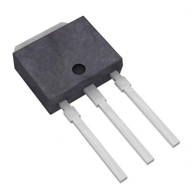
Package TO-251-3 Short Leads, IPak, TO-251AA
Category Discrete Semiconductor Products / Transistors - FETs, MOSFETs - Single
Description
Bulk Through Hole P-Channel Single Mosfet Transistor 11A Ta 11A 1W 55ns
PDF
/
Buying Options
Total Price: USD $0.74
Unit Price: USD $0.738883
≥1 USD $0.738883
≥10 USD $0.69706
≥100 USD $0.657607
≥500 USD $0.620379
≥1000 USD $0.585267
Inventory: 1136
Minimum: 1
-
+

Technical Details
Compliance
Lead Free Lead Free
RoHS Status RoHS Compliant
Radiation Hardening No
Technical
Drain to Source Breakdown Voltage -100V
Gate to Source Voltage (Vgs) 20V
Continuous Drain Current (ID) 11A
Turn-Off Delay Time 105 ns
Fall Time (Typ) 55 ns
Vgs (Max) ±20V
Drive Voltage (Max Rds On,Min Rds On) 4V 10V
Drain to Source Voltage (Vdss) 100V
Rise Time 25ns
Gate Charge (Qg) (Max) @ Vgs 21nC @ 10V
Current - Continuous Drain (Id) @ 25°C 11A Ta
Input Capacitance (Ciss) (Max) @ Vds 1020pF @ 20V
Halogen Free Halogen Free
Rds On (Max) @ Id, Vgs 275m Ω @ 5.5A, 10V
FET Type P-Channel
Turn On Delay Time 9.5 ns
Power Dissipation 1W
Element Configuration Single
Power Dissipation-Max 1W Ta 35W Tc
Number of Elements 1
Pin Count 3
Technology MOSFET (Metal Oxide)
Subcategory Other Transistors
Terminal Finish Tin/Bismuth (Sn/Bi)
ECCN Code EAR99
Moisture Sensitivity Level (MSL) 1 (Unlimited)
Part Status Obsolete
Pbfree Code yes
JESD-609 Code e6
Published 2013
Packaging Bulk
Operating Temperature 150°C TJ
Physical
Number of Pins 3
Surface Mount NO
Package / Case TO-251-3 Short Leads, IPak, TO-251AA
Mounting Type Through Hole
Supply Chain
Factory Lead Time 10 Weeks
Recommended For You

SFT1345-H+price,SFT1345-H+datasheet,SFT1345-H+in stock,buy+SFT1345-H,finder+SFT1345-H,SFT1345-H+tutorials,SFT1345-H+download