NVF2955PT1G
RoHS
/
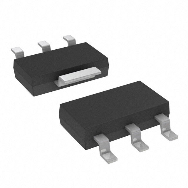
Package TO-261-4, TO-261AA
Category Discrete Semiconductor Products / Transistors - FETs, MOSFETs - Single
Description
MOSFET P CH 60V 1.7A SOT223
PDF
/
Buying Options
Total Price: USD $0.41
Unit Price: USD $0.4104
≥1 USD $0.4104
≥10 USD $0.3363
≥100 USD $0.32585
≥500 USD $0.3154
≥1000 USD $0.30495
Inventory: 1142
Minimum: 1
-
+

Technical Details
Technical
Rise Time 7.6ns
Drain to Source Voltage (Vdss) 60V
Drive Voltage (Max Rds On,Min Rds On) 10V
Vgs (Max) ±20V
Fall Time (Typ) 38 ns
Turn-Off Delay Time 65 ns
Continuous Drain Current (ID) 2.6A
Gate to Source Voltage (Vgs) 20V
Drain to Source Breakdown Voltage -60V
Avalanche Energy Rating (Eas) 225 mJ
Gate Charge (Qg) (Max) @ Vgs 14.3nC @ 10V
Current - Continuous Drain (Id) @ 25°C 1.7A Ta
Input Capacitance (Ciss) (Max) @ Vds 492pF @ 25V
Vgs(th) (Max) @ Id 4V @ 1mA
Rds On (Max) @ Id, Vgs 185m Ω @ 2.4A, 10V
Transistor Application SWITCHING
FET Type P-Channel
Turn On Delay Time 11 ns
Case Connection DRAIN
Power Dissipation 2.3W
Operating Mode ENHANCEMENT MODE
Element Configuration Single
Power Dissipation-Max 1W Ta
Number of Elements 1
Time@Peak Reflow Temperature-Max (s) 30
Peak Reflow Temperature (Cel) 260
Terminal Form GULL WING
Terminal Position DUAL
Technology MOSFET (Metal Oxide)
Terminal Finish Tin (Sn)
ECCN Code EAR99
Number of Terminations 4
Moisture Sensitivity Level (MSL) 1 (Unlimited)
Part Status Obsolete
JESD-609 Code e3
Series Automotive, AEC-Q101
Published 2008
Packaging Tape & Reel (TR)
Operating Temperature -55°C~175°C TJ
Compliance
Radiation Hardening No
RoHS Status RoHS Compliant
Physical
Transistor Element Material SILICON
Number of Pins 4
Surface Mount YES
Package / Case TO-261-4, TO-261AA
Mounting Type Surface Mount
Alternative Model

Recommended For You

NVF2955PT1G+price,NVF2955PT1G+datasheet,NVF2955PT1G+in stock,buy+NVF2955PT1G,finder+NVF2955PT1G,NVF2955PT1G+tutorials,NVF2955PT1G+download