NTNUS3171PZT5G
RoHS  RoHS compliant
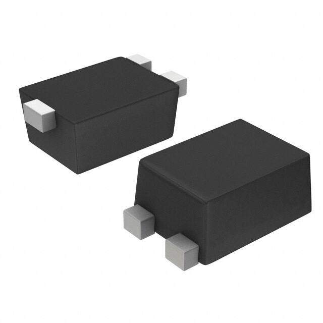
Package SOT-1123
Category Discrete Semiconductor Products / Transistors - FETs, MOSFETs - Single
Description
MOSFET T1 20V P-CH SOT-1123
PDF
/
Buying Options
Total Price: USD $1.88
Unit Price: USD $1.88425
≥1 USD $1.88425
≥10 USD $1.77759
≥100 USD $1.67697
≥500 USD $1.58205
≥1000 USD $1.4925
Inventory: 1481
Minimum: 1
-
+

Technical Details
Compliance
Lead Free Lead Free
RoHS Status ROHS3 Compliant
Dimensions
Width 650μm
Length 850μm
Height 400μm
Technical
Drain to Source Breakdown Voltage -20V
Gate to Source Voltage (Vgs) 8V
Continuous Drain Current (ID) 150mA
Turn-Off Delay Time 196 ns
Fall Time (Typ) 145 ns
Vgs (Max) ±8V
Drive Voltage (Max Rds On,Min Rds On) 1.2V 4.5V
Drain to Source Voltage (Vdss) 20V
Rise Time 56 ns
Current - Continuous Drain (Id) @ 25°C 150mA Ta
Input Capacitance (Ciss) (Max) @ Vds 13pF @ 15V
Vgs(th) (Max) @ Id 1V @ 250μA
Rds On (Max) @ Id, Vgs 3.5 Ω @ 100mA, 4.5V
Transistor Application SWITCHING
FET Type P-Channel
Turn On Delay Time 30 ns
Power Dissipation -200mW
Operating Mode ENHANCEMENT MODE
Element Configuration Single
Power Dissipation-Max 125mW Ta
Number of Elements 1
Qualification Status Not Qualified
Pin Count 3
Time@Peak Reflow Temperature-Max (s) NOT SPECIFIED
Peak Reflow Temperature (Cel) NOT SPECIFIED
Terminal Form FLAT
Terminal Position DUAL
Technology MOSFET (Metal Oxide)
Subcategory Other Transistors
Terminal Finish Tin (Sn)
ECCN Code EAR99
Number of Terminations 3
Moisture Sensitivity Level (MSL) 1 (Unlimited)
Part Status Active
Pbfree Code yes
JESD-609 Code e3
Published 2010
Packaging Tape & Reel (TR)
Operating Temperature -55°C~150°C TJ
Physical
Transistor Element Material SILICON
Number of Pins 3
Surface Mount YES
Package / Case SOT-1123
Mounting Type Surface Mount
Supply Chain
Lifecycle Status ACTIVE (Last Updated: 4 days ago)
Factory Lead Time 2 Weeks
Alternative Model

Recommended For You

NTNUS3171PZT5G+price,NTNUS3171PZT5G+datasheet,NTNUS3171PZT5G+in stock,buy+NTNUS3171PZT5G,finder+NTNUS3171PZT5G,NTNUS3171PZT5G+tutorials,NTNUS3171PZT5G+download