NTMFS4846NT1G
RoHS
/
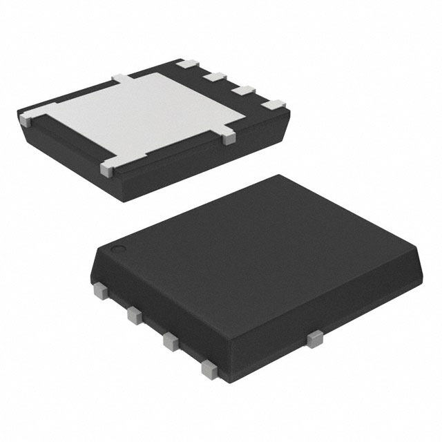
Package 8-PowerTDFN, 5 Leads
Category Discrete Semiconductor Products / Transistors - FETs, MOSFETs - Single
Description
Tape & Reel (TR) Surface Mount N-Channel Single Mosfet Transistor 12.7A Ta 100A Tc 20.3A 5.9W 7.1ns
PDF
/
Buying Options
Total Price: USD $3.27
Unit Price: USD $3.27275
≥1 USD $3.27275
≥10 USD $2.68565
≥100 USD $2.6011
≥500 USD $2.5175
≥1000 USD $2.4339
Inventory: 4676
Minimum: 1
-
+

Technical Details
Compliance
Lead Free Lead Free
RoHS Status RoHS Compliant
Radiation Hardening No
Technical
Drain to Source Breakdown Voltage 30V
Drain Current-Max (Abs) (ID) 100A
Gate to Source Voltage (Vgs) 16V
Continuous Drain Current (ID) 20.3A
Turn-Off Delay Time 34.2 ns
Fall Time (Typ) 7.1 ns
Vgs (Max) ±20V
Drive Voltage (Max Rds On,Min Rds On) 4.5V 11.5V
Rise Time 18.9ns
Gate Charge (Qg) (Max) @ Vgs 53nC @ 11.5V
Current - Continuous Drain (Id) @ 25°C 12.7A Ta 100A Tc
Input Capacitance (Ciss) (Max) @ Vds 3250pF @ 12V
Vgs(th) (Max) @ Id 2.5V @ 250μA
Rds On (Max) @ Id, Vgs 3.4m Ω @ 30A, 10V
Transistor Application SWITCHING
FET Type N-Channel
Turn On Delay Time 10.7 ns
Case Connection DRAIN
Power Dissipation 5.9W
Operating Mode ENHANCEMENT MODE
Element Configuration Single
Power Dissipation-Max 890mW Ta 55.5W Tc
Number of Elements 1
Pin Count 5
Terminal Form FLAT
Terminal Position DUAL
Technology MOSFET (Metal Oxide)
Subcategory FET General Purpose Power
ECCN Code EAR99
Number of Terminations 5
Moisture Sensitivity Level (MSL) 1 (Unlimited)
Part Status Obsolete
Pbfree Code yes
JESD-609 Code e3
Published 2009
Packaging Tape & Reel (TR)
Operating Temperature -55°C~150°C TJ
Physical
Transistor Element Material SILICON
Number of Pins 5
Surface Mount YES
Package / Case 8-PowerTDFN, 5 Leads
Mounting Type Surface Mount
Contact Plating Tin
Supply Chain
Lifecycle Status LAST SHIPMENTS (Last Updated: 1 day ago)
Recommended For You

NTMFS4846NT1G+price,NTMFS4846NT1G+datasheet,NTMFS4846NT1G+in stock,buy+NTMFS4846NT1G,finder+NTMFS4846NT1G,NTMFS4846NT1G+tutorials,NTMFS4846NT1G+download