NTMFS4821NT3G
RoHS
/
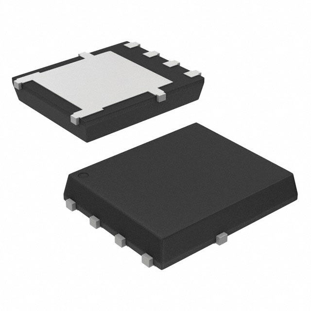
Package 8-PowerTDFN, 5 Leads
Category Discrete Semiconductor Products / Transistors - FETs, MOSFETs - Single
Description
MOSFET N-CH 30V 8.8A SO-8FL
PDF
/
Inventory: 5412
Minimum: /
The more specific your information, the faster response you will get.
Please complete the following form with the details of your request part and
contact information to get a quote.
Quotation Consultation
Technical Details
Compliance
Lead Free Lead Free
RoHS Status RoHS Compliant
Technical
Drain to Source Breakdown Voltage 30V
Drain-source On Resistance-Max 0.0108Ohm
Drain Current-Max (Abs) (ID) 100A
Gate to Source Voltage (Vgs) 16V
Continuous Drain Current (ID) 58.5A
Turn-Off Delay Time 16.6 ns
Fall Time (Typ) 3.8 ns
Vgs (Max) ±20V
Drive Voltage (Max Rds On,Min Rds On) 4.5V 10V
Rise Time 38ns
Gate Charge (Qg) (Max) @ Vgs 16nC @ 4.5V
Current - Continuous Drain (Id) @ 25°C 8.8A Ta 58.5A Tc
Input Capacitance (Ciss) (Max) @ Vds 1400pF @ 12V
Vgs(th) (Max) @ Id 2.5V @ 250μA
Rds On (Max) @ Id, Vgs 6.95m Ω @ 30A, 10V
Transistor Application SWITCHING
FET Type N-Channel
Case Connection DRAIN
Power Dissipation 38.5W
Operating Mode ENHANCEMENT MODE
Element Configuration Single
Power Dissipation-Max 870mW Ta 38.5W Tc
Number of Elements 1
Qualification Status Not Qualified
Pin Count 5
Time@Peak Reflow Temperature-Max (s) NOT SPECIFIED
Peak Reflow Temperature (Cel) NOT SPECIFIED
Terminal Form FLAT
Terminal Position DUAL
Technology MOSFET (Metal Oxide)
Subcategory FET General Purpose Power
Terminal Finish Tin (Sn)
ECCN Code EAR99
Number of Terminations 5
Moisture Sensitivity Level (MSL) 1 (Unlimited)
Part Status Obsolete
Pbfree Code yes
JESD-609 Code e3
Published 2009
Packaging Tape & Reel (TR)
Operating Temperature -55°C~150°C TJ
Physical
Transistor Element Material SILICON
Number of Pins 5
Surface Mount YES
Package / Case 8-PowerTDFN, 5 Leads
Mounting Type Surface Mount
Supply Chain
Lifecycle Status LAST SHIPMENTS (Last Updated: 1 week ago)
Alternative Model

Recommended For You

NTMFS4821NT3G+price,NTMFS4821NT3G+datasheet,NTMFS4821NT3G+in stock,buy+NTMFS4821NT3G,finder+NTMFS4821NT3G,NTMFS4821NT3G+tutorials,NTMFS4821NT3G+download