NTLJS3113PTAG
RoHS
/
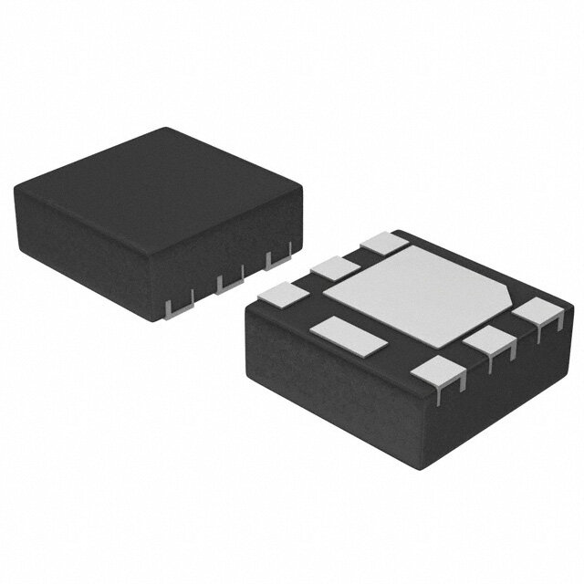
Package 6-WDFN Exposed Pad
Category Discrete Semiconductor Products / Transistors - FETs, MOSFETs - Single
Description
MOSFET P-CH 20V 3.5A 6-WDFN
PDF
/
Buying Options
Total Price: USD $1.81
Unit Price: USD $1.80595
≥1 USD $1.80595
≥10 USD $1.482
≥100 USD $1.43545
≥500 USD $1.38985
≥1000 USD $1.3433
Inventory: 1097
Minimum: 1
-
+

Technical Details
Compliance
Lead Free Lead Free
RoHS Status RoHS Compliant
Radiation Hardening No
Technical
Pulsed Drain Current-Max (IDM) 23A
Drain to Source Breakdown Voltage 20V
Drain Current-Max (Abs) (ID) 3.5A
Gate to Source Voltage (Vgs) 8V
Continuous Drain Current (ID) -5.8A
Turn-Off Delay Time 60 ns
Fall Time (Typ) 17.5 ns
Vgs (Max) ±8V
Drive Voltage (Max Rds On,Min Rds On) 1.5V 4.5V
Rise Time 17.5 ns
Gate Charge (Qg) (Max) @ Vgs 15.7nC @ 4.5V
Current - Continuous Drain (Id) @ 25°C 3.5A Ta
Input Capacitance (Ciss) (Max) @ Vds 1329pF @ 16V
Vgs(th) (Max) @ Id 1V @ 250μA
Rds On (Max) @ Id, Vgs 40m Ω @ 3A, 4.5V
Transistor Application SWITCHING
FET Type P-Channel
Turn On Delay Time 6.9 ns
Case Connection DRAIN
Power Dissipation 1.9W
Operating Mode ENHANCEMENT MODE
Element Configuration Single
Power Dissipation-Max 700mW Ta
Number of Elements 1
Pin Count 6
Terminal Form C BEND
Terminal Position DUAL
Technology MOSFET (Metal Oxide)
Subcategory Other Transistors
Additional Feature LOGIC LEVEL COMPATIBLE
Terminal Finish Tin (Sn)
Resistance 40MOhm
ECCN Code EAR99
Number of Terminations 6
Moisture Sensitivity Level (MSL) 1 (Unlimited)
Part Status Obsolete
Pbfree Code yes
JESD-609 Code e3
Published 2007
Packaging Tape & Reel (TR)
Operating Temperature -55°C~150°C TJ
Physical
Transistor Element Material SILICON
Number of Pins 6
Surface Mount YES
Package / Case 6-WDFN Exposed Pad
Mounting Type Surface Mount
Supply Chain
Lifecycle Status ACTIVE (Last Updated: 1 week ago)
Factory Lead Time 5 Weeks
Alternative Model

Recommended For You

NTLJS3113PTAG+price,NTLJS3113PTAG+datasheet,NTLJS3113PTAG+in stock,buy+NTLJS3113PTAG,finder+NTLJS3113PTAG,NTLJS3113PTAG+tutorials,NTLJS3113PTAG+download