NTHD5904NT3
RoHS
/
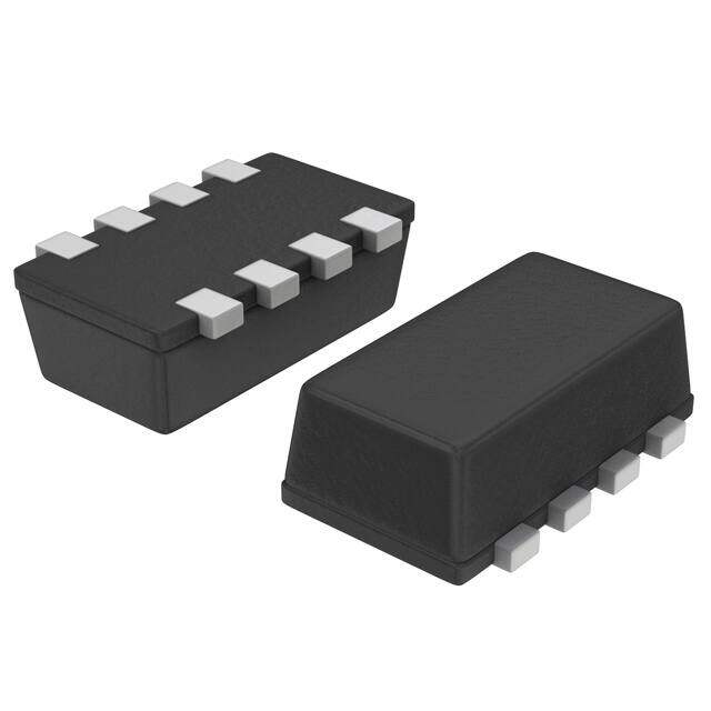
Package 8-SMD, Flat Lead
Category Discrete Semiconductor Products / Transistors - FETs, MOSFETs - Single
Description
MOSFET N-CH 20V 2.5A CHIPFET
PDF
/
Inventory: 5494
Minimum: /
The more specific your information, the faster response you will get.
Please complete the following form with the details of your request part and
contact information to get a quote.
Quotation Consultation
Technical Details
Compliance
Lead Free Contains Lead
RoHS Status Non-RoHS Compliant
Technical
Drain to Source Breakdown Voltage 20V
Drain-source On Resistance-Max 0.065Ohm
Gate to Source Voltage (Vgs) 8V
Continuous Drain Current (ID) 2.5A
Turn-Off Delay Time 17 ns
Fall Time (Typ) 17 ns
Vgs (Max) ±8V
Drive Voltage (Max Rds On,Min Rds On) 2.5V 4.5V
Rise Time 17ns
Gate Charge (Qg) (Max) @ Vgs 6nC @ 4.5V
Current - Continuous Drain (Id) @ 25°C 2.5A Ta
Input Capacitance (Ciss) (Max) @ Vds 465pF @ 16V
Vgs(th) (Max) @ Id 1.2V @ 250μA
Rds On (Max) @ Id, Vgs 65m Ω @ 3.3A, 4.5V
Transistor Application SWITCHING
FET Type N-Channel
Power Dissipation 1.13W
Operating Mode ENHANCEMENT MODE
Element Configuration Dual
Power Dissipation-Max 640mW Ta
Number of Elements 2
Qualification Status Not Qualified
Pin Count 8
Time@Peak Reflow Temperature-Max (s) 30
Current Rating 3.3A
Reach Compliance Code not_compliant
Peak Reflow Temperature (Cel) 240
Terminal Form C BEND
Technology MOSFET (Metal Oxide)
Voltage - Rated DC 20V
Subcategory FET General Purpose Power
Terminal Finish Tin/Lead (Sn/Pb)
ECCN Code EAR99
Number of Terminations 8
Moisture Sensitivity Level (MSL) 3 (168 Hours)
Part Status Obsolete
JESD-609 Code e0
Published 2005
Packaging Tape & Reel (TR)
Operating Temperature -55°C~150°C TJ
Physical
Transistor Element Material SILICON
Number of Pins 8
Package / Case 8-SMD, Flat Lead
Mounting Type Surface Mount
Mount Surface Mount
Alternative Model

Recommended For You

NTHD5904NT3+price,NTHD5904NT3+datasheet,NTHD5904NT3+in stock,buy+NTHD5904NT3,finder+NTHD5904NT3,NTHD5904NT3+tutorials,NTHD5904NT3+download