NTHD3101FT1G
RoHS  RoHS compliant
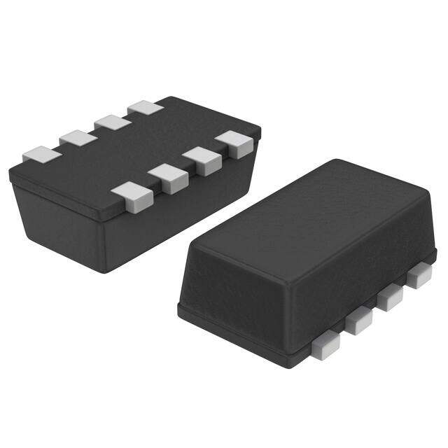
Package 8-SMD, Flat Lead
Category Discrete Semiconductor Products / Transistors - FETs, MOSFETs - Single
Description
P-Channel 20 V 64 mOhm 1.1 W Surface Mount Power MOSFET - CASE 1206A
PDF
/
Buying Options
Total Price: USD $0.46
Unit Price: USD $0.461023
≥1 USD $0.461023
≥10 USD $0.439067
≥100 USD $0.418801
Inventory: 1199
Minimum: 1
-
+

Technical Details
Compliance
Lead Free Lead Free
RoHS Status ROHS3 Compliant
REACH SVHC No SVHC
Radiation Hardening No
Dimensions
Width 1.65mm
Length 3.05mm
Height 1.05mm
Technical
Nominal Vgs -450 mV
FET Feature Schottky Diode (Isolated)
Drain to Source Breakdown Voltage -20V
Gate to Source Voltage (Vgs) 8V
Threshold Voltage -1.5V
Continuous Drain Current (ID) 4.4A
Turn-Off Delay Time 16 ns
Fall Time (Typ) 12.4 ns
Vgs (Max) ±8V
Drive Voltage (Max Rds On,Min Rds On) 1.8V 4.5V
Drain to Source Voltage (Vdss) 20V
Rise Time 11.7 ns
Gate Charge (Qg) (Max) @ Vgs 7.4nC @ 4.5V
Current - Continuous Drain (Id) @ 25°C 3.2A Tj
Input Capacitance (Ciss) (Max) @ Vds 680pF @ 10V
Vgs(th) (Max) @ Id 1.5V @ 250μA
Rds On (Max) @ Id, Vgs 80m Ω @ 3.2A, 4.5V
Transistor Application SWITCHING
FET Type P-Channel
Turn On Delay Time 5.8 ns
Power Dissipation 1.1W
Operating Mode ENHANCEMENT MODE
Power Dissipation-Max 1.1W Ta
Configuration SINGLE WITH BUILT-IN DIODE
Number of Elements 1
Pin Count 8
Time@Peak Reflow Temperature-Max (s) 40
Current Rating -3.2A
Peak Reflow Temperature (Cel) 260
Terminal Form C BEND
Terminal Position DUAL
Technology MOSFET (Metal Oxide)
Voltage - Rated DC -20V
Subcategory Other Transistors
Resistance 64MOhm
ECCN Code EAR99
Number of Terminations 8
Moisture Sensitivity Level (MSL) 1 (Unlimited)
Part Status Active
Pbfree Code yes
JESD-609 Code e3
Published 2006
Packaging Tape & Reel (TR)
Operating Temperature -55°C~150°C TJ
Physical
Transistor Element Material SILICON
Weight 4.535924g
Number of Pins 8
Surface Mount YES
Package / Case 8-SMD, Flat Lead
Mounting Type Surface Mount
Contact Plating Tin
Supply Chain
Lifecycle Status ACTIVE (Last Updated: 2 hours ago)
Factory Lead Time 5 Weeks
Alternative Model

Recommended For You

NTHD3101FT1G+price,NTHD3101FT1G+datasheet,NTHD3101FT1G+in stock,buy+NTHD3101FT1G,finder+NTHD3101FT1G,NTHD3101FT1G+tutorials,NTHD3101FT1G+download