NTD4858N-35G
RoHS  RoHS compliant
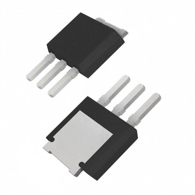
Package TO-251-3 Stub Leads, IPak
Category Discrete Semiconductor Products / Transistors - FETs, MOSFETs - Single
Description
MOSFET NFET 25V 73A 0.0062R DPAK
PDF
/
Buying Options
Total Price: USD $0.81
Unit Price: USD $0.8096
≥1 USD $0.8096
≥10 USD $0.64885
≥100 USD $0.51421
≥500 USD $0.435864
Inventory: 771
Minimum: 1
-
+

Technical Details
Compliance
Lead Free Lead Free
RoHS Status ROHS3 Compliant
Radiation Hardening No
Technical
Drain to Source Breakdown Voltage 25V
Gate to Source Voltage (Vgs) 20V
Continuous Drain Current (ID) 13.6A
Turn-Off Delay Time 23.8 ns
Fall Time (Typ) 2.8 ns
Vgs (Max) ±20V
Drive Voltage (Max Rds On,Min Rds On) 4.5V 10V
Rise Time 17.3ns
Gate Charge (Qg) (Max) @ Vgs 19.2nC @ 4.5V
Current - Continuous Drain (Id) @ 25°C 11.2A Ta 73A Tc
Input Capacitance (Ciss) (Max) @ Vds 1563pF @ 12V
Vgs(th) (Max) @ Id 2.5V @ 250μA
Rds On (Max) @ Id, Vgs 6.2m Ω @ 30A, 10V
Transistor Application SWITCHING
FET Type N-Channel
Case Connection DRAIN
Power Dissipation 2W
Operating Mode ENHANCEMENT MODE
Element Configuration Single
Power Dissipation-Max 1.3W Ta 54.5W Tc
Number of Elements 1
Pin Count 3
Technology MOSFET (Metal Oxide)
Subcategory FET General Purpose Power
Terminal Finish Tin (Sn)
ECCN Code EAR99
Number of Terminations 3
Moisture Sensitivity Level (MSL) 1 (Unlimited)
Part Status Active
Pbfree Code yes
JESD-609 Code e3
Published 2007
Packaging Tube
Operating Temperature -55°C~175°C TJ
Physical
Transistor Element Material SILICON
Number of Pins 3
Surface Mount NO
Package / Case TO-251-3 Stub Leads, IPak
Mounting Type Through Hole
Supply Chain
Lifecycle Status ACTIVE (Last Updated: 1 day ago)
Factory Lead Time 4 Weeks
Alternative Model

Recommended For You

NTD4858N-35G+price,NTD4858N-35G+datasheet,NTD4858N-35G+in stock,buy+NTD4858N-35G,finder+NTD4858N-35G,NTD4858N-35G+tutorials,NTD4858N-35G+download