NTB60N06LT4
RoHS
/
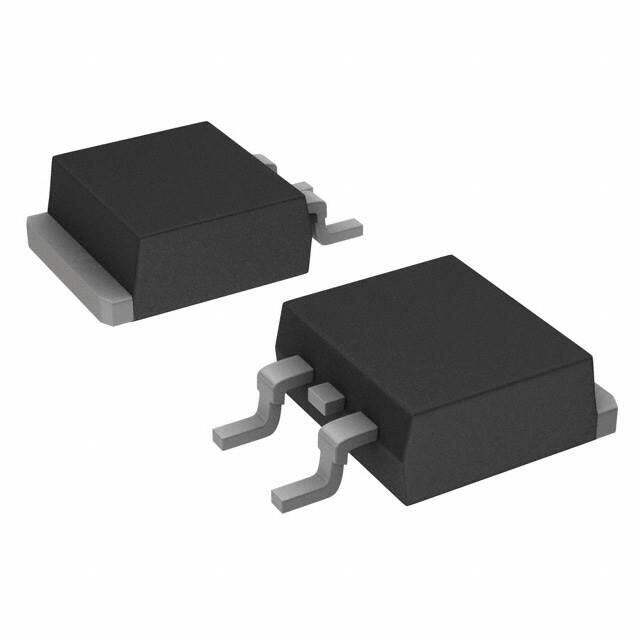
Package TO-263-3, D2Pak (2 Leads + Tab), TO-263AB
Category Discrete Semiconductor Products / Transistors - FETs, MOSFETs - Single
Description
MOSFET N-CH 60V 60A D2PAK
PDF
/
Buying Options
Total Price: USD $12.11
Unit Price: USD $12.1068
≥1 USD $12.1068
≥10 USD $9.93415
≥100 USD $9.6235
≥500 USD $9.31285
≥1000 USD $9.0022
Inventory: 1402
Minimum: 1
-
+

Technical Details
Technical
ECCN Code EAR99
Terminal Finish Tin/Lead (Sn/Pb)
Additional Feature LOGIC LEVEL COMPATIBLE
Subcategory FET General Purpose Power
Voltage - Rated DC 60V
Technology MOSFET (Metal Oxide)
Terminal Form GULL WING
Peak Reflow Temperature (Cel) 240
Reach Compliance Code not_compliant
Current Rating 60A
Time@Peak Reflow Temperature-Max (s) 30
Pin Count 3
JESD-30 Code R-PSSO-G2
Qualification Status Not Qualified
Number of Elements 1
Power Dissipation-Max 2.4W Ta 150W Tj
Element Configuration Single
Operating Mode ENHANCEMENT MODE
Power Dissipation 150W
Case Connection DRAIN
FET Type N-Channel
Transistor Application SWITCHING
Rds On (Max) @ Id, Vgs 16m Ω @ 30A, 5V
Vgs(th) (Max) @ Id 2V @ 250μA
Input Capacitance (Ciss) (Max) @ Vds 3075pF @ 25V
Current - Continuous Drain (Id) @ 25°C 60A Ta
Gate Charge (Qg) (Max) @ Vgs 65nC @ 5V
Rise Time 576ns
Drive Voltage (Max Rds On,Min Rds On) 5V
Vgs (Max) ±15V
Fall Time (Typ) 237 ns
Turn-Off Delay Time 100 ns
Number of Terminations 2
Moisture Sensitivity Level (MSL) 1 (Unlimited)
Part Status Obsolete
Pbfree Code no
JESD-609 Code e0
Published 2005
Packaging Tape & Reel (TR)
Operating Temperature -55°C~175°C TJ
Continuous Drain Current (ID) 60A
Gate to Source Voltage (Vgs) 15V
Drain-source On Resistance-Max 0.016Ohm
Drain to Source Breakdown Voltage 60V
Pulsed Drain Current-Max (IDM) 180A
Avalanche Energy Rating (Eas) 454 mJ
Physical
Transistor Element Material SILICON
Number of Pins 3
Package / Case TO-263-3, D2Pak (2 Leads + Tab), TO-263AB
Mounting Type Surface Mount
Mount Surface Mount
Supply Chain
Lifecycle Status LAST SHIPMENTS (Last Updated: 6 days ago)
Compliance
RoHS Status Non-RoHS Compliant
Lead Free Contains Lead
Alternative Model

Recommended For You

NTB60N06LT4+price,NTB60N06LT4+datasheet,NTB60N06LT4+in stock,buy+NTB60N06LT4,finder+NTB60N06LT4,NTB60N06LT4+tutorials,NTB60N06LT4+download