MTB50P03HDLT4G
RoHS  RoHS compliant
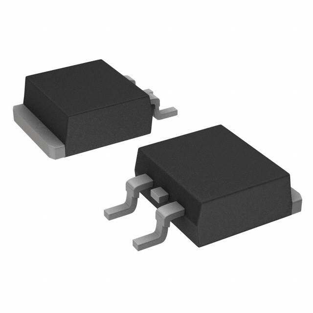
Package TO-263-3, D2Pak (2 Leads + Tab), TO-263AB
Category Discrete Semiconductor Products / Transistors - FETs, MOSFETs - Single
Description
MOSFET PFET D2PAK 30V 50A 25mOhm
PDF
/
Buying Options
Total Price: USD $31.14
Unit Price: USD $31.14385
≥1 USD $31.14385
≥10 USD $25.55405
≥100 USD $24.7551
≥500 USD $23.9571
≥1000 USD $23.15815
≥3000 USD $20.7632
Inventory: 77
Minimum: 1
-
+

Technical Details
Compliance
Lead Free Lead Free
RoHS Status ROHS3 Compliant
REACH SVHC No SVHC
Radiation Hardening No
Dimensions
Width 9.65mm
Length 10.29mm
Height 4.83mm
Technical
Drain to Source Breakdown Voltage -30V
Gate to Source Voltage (Vgs) 15V
Threshold Voltage 1.5V
Continuous Drain Current (ID) 50A
Turn-Off Delay Time 90 ns
Fall Time (Typ) 218 ns
Vgs (Max) ±15V
Drive Voltage (Max Rds On,Min Rds On) 5V
Drain to Source Voltage (Vdss) 30V
Rise Time 340 ns
Gate Charge (Qg) (Max) @ Vgs 100nC @ 5V
Current - Continuous Drain (Id) @ 25°C 50A Tc
Input Capacitance (Ciss) (Max) @ Vds 4900pF @ 25V
Vgs(th) (Max) @ Id 2V @ 250μA
Rds On (Max) @ Id, Vgs 25m Ω @ 25A, 5V
Transistor Application SWITCHING
FET Type P-Channel
Turn On Delay Time 22 ns
Case Connection DRAIN
Power Dissipation 125W
Operating Mode ENHANCEMENT MODE
Element Configuration Single
Power Dissipation-Max 2.5W Ta 125W Tc
Number of Elements 1
JESD-30 Code R-PSSO-G2
Pin Count 3
Time@Peak Reflow Temperature-Max (s) 40
Current Rating -50A
Peak Reflow Temperature (Cel) 260
Terminal Form GULL WING
Technology MOSFET (Metal Oxide)
Voltage - Rated DC -30V
Subcategory Other Transistors
Additional Feature AVALANCHE RATED
Resistance 25MOhm
ECCN Code EAR99
Number of Terminations 2
Moisture Sensitivity Level (MSL) 1 (Unlimited)
Part Status Not For New Designs
Pbfree Code yes
JESD-609 Code e3
Published 2006
Packaging Tape & Reel (TR)
Operating Temperature -55°C~150°C TJ
Physical
Transistor Element Material SILICON
Number of Pins 3
Surface Mount YES
Package / Case TO-263-3, D2Pak (2 Leads + Tab), TO-263AB
Mounting Type Surface Mount
Contact Plating Tin
Supply Chain
Lifecycle Status ACTIVE, NOT REC (Last Updated: 3 days ago)
Factory Lead Time 17 Weeks
Alternative Model

Recommended For You

MTB50P03HDLT4G+price,MTB50P03HDLT4G+datasheet,MTB50P03HDLT4G+in stock,buy+MTB50P03HDLT4G,finder+MTB50P03HDLT4G,MTB50P03HDLT4G+tutorials,MTB50P03HDLT4G+download