FQB19N20CTM
RoHS  RoHS compliant
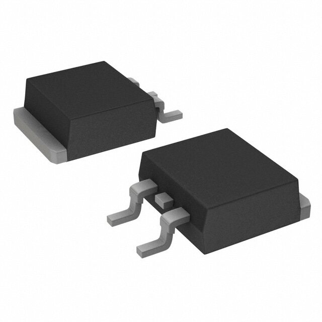
Package TO-263-3, D2Pak (2 Leads + Tab), TO-263AB
Category Discrete Semiconductor Products / Transistors - FETs, MOSFETs - Single
Description
MOSFET N-CH 200V 19A D2PAK
PDF
/
Buying Options
Total Price: USD $1.33
Unit Price: USD $1.32715
≥1 USD $1.32715
≥10 USD $1.08965
≥100 USD $1.05545
≥500 USD $1.02125
≥1000 USD $0.98705
Inventory: 15007
Minimum: 1
-
+

Technical Details
Compliance
Lead Free Lead Free
RoHS Status ROHS3 Compliant
Radiation Hardening No
Dimensions
Width 9.65mm
Length 10.67mm
Height 4.83mm
Technical
Pulsed Drain Current-Max (IDM) 76A
Drain to Source Breakdown Voltage 200V
Gate to Source Voltage (Vgs) 30V
Continuous Drain Current (ID) 19A
Turn-Off Delay Time 135 ns
Fall Time (Typ) 115 ns
Vgs (Max) ±30V
Drive Voltage (Max Rds On,Min Rds On) 10V
Rise Time 150 ns
Gate Charge (Qg) (Max) @ Vgs 53nC @ 10V
Current - Continuous Drain (Id) @ 25°C 19A Tc
Input Capacitance (Ciss) (Max) @ Vds 1080pF @ 25V
Vgs(th) (Max) @ Id 4V @ 250μA
Rds On (Max) @ Id, Vgs 170m Ω @ 9.5A, 10V
Transistor Application SWITCHING
FET Type N-Channel
Turn On Delay Time 15 ns
Case Connection DRAIN
Power Dissipation 3.13W
Operating Mode ENHANCEMENT MODE
Element Configuration Single
Power Dissipation-Max 3.13W Ta 139W Tc
Number of Elements 1
JESD-30 Code R-PSSO-G2
Current Rating 19A
Terminal Form GULL WING
Technology MOSFET (Metal Oxide)
Voltage - Rated DC 200V
Subcategory FET General Purpose Power
HTS Code 8541.29.00.95
Terminal Finish Tin (Sn)
Resistance 170mOhm
ECCN Code EAR99
Number of Terminations 2
Moisture Sensitivity Level (MSL) 1 (Unlimited)
Part Status Active
Pbfree Code yes
JESD-609 Code e3
Series QFET?
Published 2004
Packaging Tape & Reel (TR)
Operating Temperature -55°C~150°C TJ
Physical
Transistor Element Material SILICON
Weight 1.31247g
Number of Pins 3
Package / Case TO-263-3, D2Pak (2 Leads + Tab), TO-263AB
Mounting Type Surface Mount
Mount Surface Mount
Supply Chain
Lifecycle Status ACTIVE (Last Updated: 16 hours ago)
Factory Lead Time 5 Weeks
Alternative Model

Recommended For You

FQB19N20CTM+price,FQB19N20CTM+datasheet,FQB19N20CTM+in stock,buy+FQB19N20CTM,finder+FQB19N20CTM,FQB19N20CTM+tutorials,FQB19N20CTM+download