FQA38N30
RoHS
/
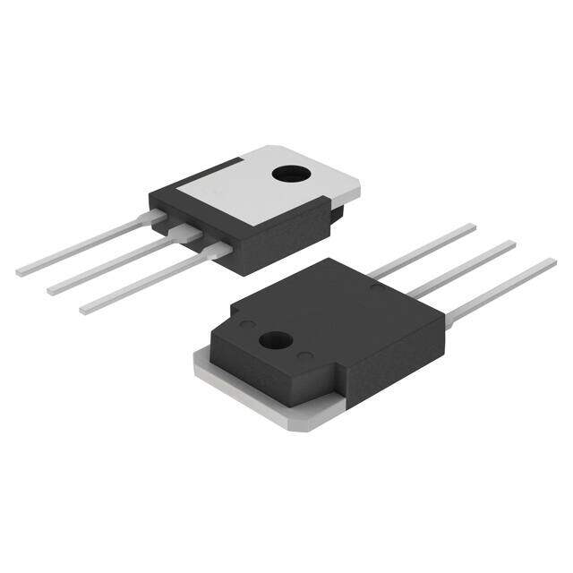
Package TO-3P-3, SC-65-3
Category Discrete Semiconductor Products / Transistors - FETs, MOSFETs - Single
Description
MOSFET N-CH 300V 38.4A TO-3P
PDF
/
Buying Options
Total Price: USD $3.22
Unit Price: USD $3.2224
≥1 USD $3.2224
≥10 USD $2.64385
≥100 USD $2.5612
≥500 USD $2.47855
≥1000 USD $2.3959
Inventory: 6017
Minimum: 1
-
+

Technical Details
Compliance
Lead Free Lead Free
RoHS Status RoHS Compliant
Dimensions
Width 5mm
Length 15.8mm
Height 18.9mm
Technical
Drain to Source Breakdown Voltage 300V
Drain-source On Resistance-Max 0.085Ohm
Gate to Source Voltage (Vgs) 30V
Continuous Drain Current (ID) 38.4A
Turn-Off Delay Time 170 ns
Fall Time (Typ) 190 ns
Vgs (Max) ±30V
Drive Voltage (Max Rds On,Min Rds On) 10V
Rise Time 430 ns
Gate Charge (Qg) (Max) @ Vgs 120nC @ 10V
Current - Continuous Drain (Id) @ 25°C 38.4A Tc
Input Capacitance (Ciss) (Max) @ Vds 4400pF @ 25V
Vgs(th) (Max) @ Id 5V @ 250μA
Rds On (Max) @ Id, Vgs 85m Ω @ 19.2A, 10V
Transistor Application SWITCHING
FET Type N-Channel
Turn On Delay Time 80 ns
Power Dissipation 290W
Operating Mode ENHANCEMENT MODE
Element Configuration Single
Power Dissipation-Max 290W Tc
Number of Elements 1
Qualification Status Not Qualified
Time@Peak Reflow Temperature-Max (s) NOT SPECIFIED
Current Rating 38.4A
Peak Reflow Temperature (Cel) NOT SPECIFIED
Technology MOSFET (Metal Oxide)
Voltage - Rated DC 300V
Terminal Finish Tin (Sn)
ECCN Code EAR99
Number of Terminations 3
Moisture Sensitivity Level (MSL) 1 (Unlimited)
Part Status Obsolete
Pbfree Code yes
JESD-609 Code e3
Series QFET?
Published 2000
Packaging Tube
Operating Temperature -55°C~150°C TJ
Physical
Transistor Element Material SILICON
Weight 6.401g
Number of Pins 3
Package / Case TO-3P-3, SC-65-3
Mounting Type Through Hole
Mount Through Hole
Supply Chain
Lifecycle Status ACTIVE, NOT REC (Last Updated: 1 week ago)
Factory Lead Time 4 Weeks
Alternative Model

Recommended For You

FQA38N30+price,FQA38N30+datasheet,FQA38N30+in stock,buy+FQA38N30,finder+FQA38N30,FQA38N30+tutorials,FQA38N30+download