FDS3580
RoHS  RoHS compliant
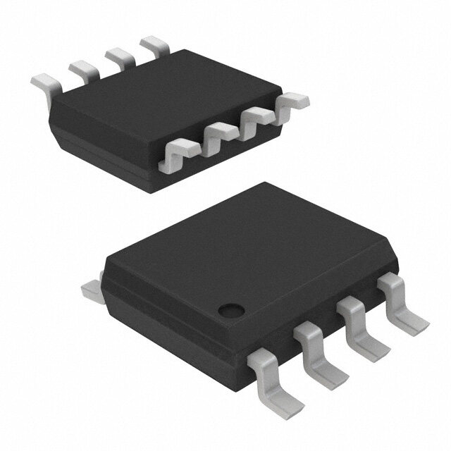
Package 8-SOIC (0.154, 3.90mm Width)
Category Discrete Semiconductor Products / Transistors - FETs, MOSFETs - Single
Description
MOSFET SO-8 N-CH 80V
PDF
/
Buying Options
Total Price: USD $1.37
Unit Price: USD $1.3728
≥1 USD $1.3728
≥10 USD $1.12112
≥100 USD $0.87164
≥500 USD $0.73883
≥1000 USD $0.60185
Inventory: 1144
Minimum: 1
-
+

Technical Details
Compliance
Lead Free Lead Free
RoHS Status ROHS3 Compliant
Radiation Hardening No
Dimensions
Width 3.9mm
Length 4.9mm
Height 1.575mm
Technical
Drain to Source Breakdown Voltage 80V
Gate to Source Voltage (Vgs) 20V
Continuous Drain Current (ID) 7.6A
Turn-Off Delay Time 34 ns
Fall Time (Typ) 16 ns
Vgs (Max) ±20V
Drive Voltage (Max Rds On,Min Rds On) 6V 10V
Rise Time 8 ns
Gate Charge (Qg) (Max) @ Vgs 46nC @ 10V
Current - Continuous Drain (Id) @ 25°C 7.6A Ta
Input Capacitance (Ciss) (Max) @ Vds 1800pF @ 25V
Vgs(th) (Max) @ Id 4V @ 250μA
Rds On (Max) @ Id, Vgs 29m Ω @ 7.6A, 10V
Transistor Application SWITCHING
FET Type N-Channel
Turn On Delay Time 13 ns
Power Dissipation 2.5W
Operating Mode ENHANCEMENT MODE
Element Configuration Single
Power Dissipation-Max 2.5W Ta
Number of Elements 1
Current Rating 7.6A
Terminal Form GULL WING
Terminal Position DUAL
Technology MOSFET (Metal Oxide)
Voltage - Rated DC 80V
Subcategory FET General Purpose Power
Terminal Finish Tin (Sn)
Resistance 29mOhm
ECCN Code EAR99
Number of Terminations 8
Moisture Sensitivity Level (MSL) 1 (Unlimited)
Part Status Active
Pbfree Code yes
JESD-609 Code e3
Series PowerTrench?
Published 2000
Packaging Tape & Reel (TR)
Operating Temperature -55°C~150°C TJ
Physical
Transistor Element Material SILICON
Weight 130mg
Number of Pins 8
Package / Case 8-SOIC (0.154, 3.90mm Width)
Mounting Type Surface Mount
Mount Surface Mount
Supply Chain
Lifecycle Status ACTIVE (Last Updated: 1 day ago)
Factory Lead Time 11 Weeks
Alternative Model

Recommended For You

FDS3580+price,FDS3580+datasheet,FDS3580+in stock,buy+FDS3580,finder+FDS3580,FDS3580+tutorials,FDS3580+download