FDPF5N50UT
RoHS  RoHS compliant
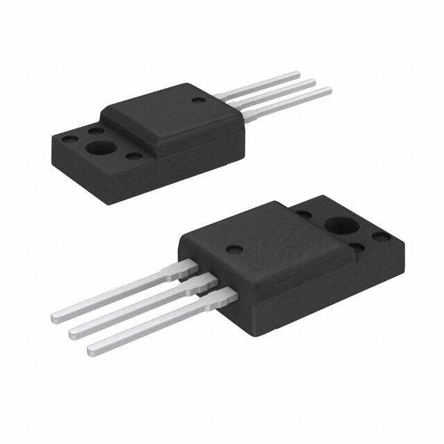
Package TO-220-3 Full Pack
Category Discrete Semiconductor Products / Transistors - FETs, MOSFETs - Single
Description
MOSFET 500V N-Channel FRFET, Ultra FRFET
PDF
/
Buying Options
Total Price: USD $0.56
Unit Price: USD $0.5632
≥1 USD $0.5632
Inventory: 20668
Minimum: 1
-
+

Technical Details
Compliance
RoHS Status ROHS3 Compliant
Dimensions
Width 4.9mm
Length 10.36mm
Height 16.07mm
Technical
Drain to Source Breakdown Voltage 500V
Drain-source On Resistance-Max 2Ohm
Drain Current-Max (Abs) (ID) 4A
Gate to Source Voltage (Vgs) 30V
JEDEC-95 Code TO-220AB
Continuous Drain Current (ID) 4A
Turn-Off Delay Time 27 ns
Fall Time (Typ) 20 ns
Vgs (Max) ±30V
Drive Voltage (Max Rds On,Min Rds On) 10V
Rise Time 21 ns
Gate Charge (Qg) (Max) @ Vgs 15nC @ 10V
Current - Continuous Drain (Id) @ 25°C 4A Tc
Input Capacitance (Ciss) (Max) @ Vds 650pF @ 25V
Vgs(th) (Max) @ Id 5V @ 250μA
Rds On (Max) @ Id, Vgs 2 Ω @ 2A, 10V
Transistor Application SWITCHING
FET Type N-Channel
Turn On Delay Time 14 ns
Case Connection ISOLATED
Power Dissipation 28W
Operating Mode ENHANCEMENT MODE
Element Configuration Single
Power Dissipation-Max 28W Tc
Number of Elements 1
Qualification Status Not Qualified
Time@Peak Reflow Temperature-Max (s) NOT SPECIFIED
Reach Compliance Code not_compliant
Peak Reflow Temperature (Cel) NOT SPECIFIED
Technology MOSFET (Metal Oxide)
Subcategory FET General Purpose Power
Terminal Finish Tin (Sn)
ECCN Code EAR99
Number of Terminations 3
Moisture Sensitivity Level (MSL) 1 (Unlimited)
Part Status Active
Pbfree Code yes
JESD-609 Code e3
Series FRFET?
Published 2013
Packaging Tube
Operating Temperature -55°C~150°C TJ
Physical
Transistor Element Material SILICON
Weight 2.27g
Number of Pins 3
Package / Case TO-220-3 Full Pack
Mounting Type Through Hole
Mount Through Hole
Supply Chain
Lifecycle Status ACTIVE (Last Updated: 6 days ago)
Factory Lead Time 7 Weeks
Alternative Model

Recommended For You

FDPF5N50UT+price,FDPF5N50UT+datasheet,FDPF5N50UT+in stock,buy+FDPF5N50UT,finder+FDPF5N50UT,FDPF5N50UT+tutorials,FDPF5N50UT+download