FDP3652
RoHS  RoHS compliant
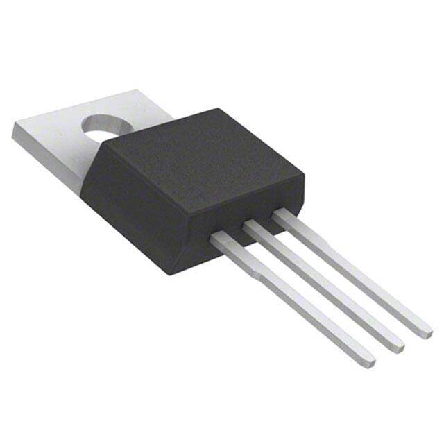
Package TO-220-3
Category Discrete Semiconductor Products / Transistors - FETs, MOSFETs - Single
Description
Trans MOSFET N-CH 100V 9A Automotive 3-Pin(3+Tab) TO-220AB Tube
PDF
/
Buying Options
Total Price: USD $1.61
Unit Price: USD $1.6104
≥1 USD $1.6104
≥10 USD $1.33672
≥100 USD $1.064008
≥500 USD $0.900293
≥1000 USD $0.763893
≥3000 USD $0.725692
Inventory: 598
Minimum: 1
-
+

Technical Details
Compliance
Lead Free Lead Free
RoHS Status ROHS3 Compliant
REACH SVHC No SVHC
Radiation Hardening No
Dimensions
Width 4.83mm
Length 10.67mm
Height 9.4mm
Technical
Drain to Source Breakdown Voltage 100V
Drain Current-Max (Abs) (ID) 9A
Gate to Source Voltage (Vgs) 20V
JEDEC-95 Code TO-220AB
Threshold Voltage 4V
Continuous Drain Current (ID) 61A
Turn-Off Delay Time 26 ns
Fall Time (Typ) 45 ns
Vgs (Max) ±20V
Drive Voltage (Max Rds On,Min Rds On) 6V 10V
Rise Time 85 ns
Gate Charge (Qg) (Max) @ Vgs 53nC @ 10V
Current - Continuous Drain (Id) @ 25°C 9A Ta 61A Tc
Input Capacitance (Ciss) (Max) @ Vds 2880pF @ 25V
Vgs(th) (Max) @ Id 4V @ 250μA
Rds On (Max) @ Id, Vgs 16m Ω @ 61A, 10V
Transistor Application SWITCHING
FET Type N-Channel
Turn On Delay Time 12 ns
Case Connection DRAIN
Power Dissipation 150W
Operating Mode ENHANCEMENT MODE
Element Configuration Single
Power Dissipation-Max 150W Tc
Number of Elements 1
Current Rating 61A
Technology MOSFET (Metal Oxide)
Voltage - Rated DC 100V
Terminal Finish Tin (Sn)
Resistance 16MOhm
ECCN Code EAR99
Number of Terminations 3
Moisture Sensitivity Level (MSL) 1 (Unlimited)
Part Status Not For New Designs
Pbfree Code yes
JESD-609 Code e3
Series PowerTrench?
Published 2003
Packaging Bulk
Operating Temperature -55°C~175°C TJ
Physical
Transistor Element Material SILICON
Weight 1.8g
Number of Pins 3
Package / Case TO-220-3
Mounting Type Through Hole
Mount Through Hole
Supply Chain
Lifecycle Status ACTIVE, NOT REC (Last Updated: 3 days ago)
Alternative Model

Recommended For You

FDP3652+price,FDP3652+datasheet,FDP3652+in stock,buy+FDP3652,finder+FDP3652,FDP3652+tutorials,FDP3652+download