FDMS86255
RoHS  RoHS compliant
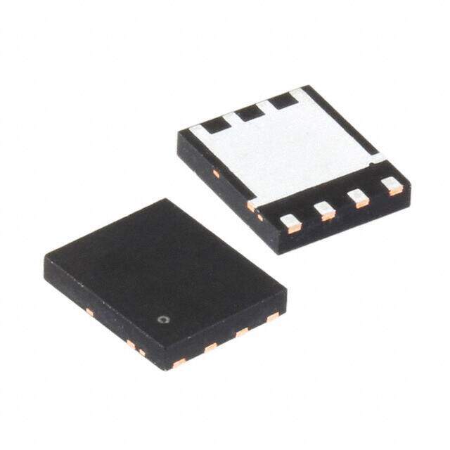
Package 8-PowerTDFN
Category Discrete Semiconductor Products / Transistors - FETs, MOSFETs - Single
Description
PT5 150V/20V Nch PowerTrench MOSFET - 8LD, PQFN, POWERCLIP SINGLE, JEDEC, MO-240, VARIATION AA, 5.
PDF
/
Buying Options
Total Price: USD $3.67
Unit Price: USD $3.6696
≥1 USD $3.6696
≥10 USD $3.08264
≥100 USD $2.493832
≥500 USD $2.216738
≥1000 USD $1.898081
Inventory: 1211
Minimum: 1
-
+

Technical Details
Compliance
RoHS Status ROHS3 Compliant
Dimensions
Width 6.25mm
Length 5.1mm
Height 1.1mm
Technical
Max Junction Temperature (Tj) 150°C
Drain to Source Breakdown Voltage 150V
Drain Current-Max (Abs) (ID) 45A
Gate to Source Voltage (Vgs) 20V
JEDEC-95 Code MO-240AA
Continuous Drain Current (ID) 10A
Turn-Off Delay Time 28 ns
Fall Time (Typ) 12 ns
Vgs (Max) ±20V
Drive Voltage (Max Rds On,Min Rds On) 6V 10V
Rise Time 10 ns
Gate Charge (Qg) (Max) @ Vgs 63nC @ 10V
Current - Continuous Drain (Id) @ 25°C 10A Ta 45A Tc
Input Capacitance (Ciss) (Max) @ Vds 4480pF @ 75V
Vgs(th) (Max) @ Id 4V @ 250μA
Rds On (Max) @ Id, Vgs 12.4m Ω @ 10A, 10V
Transistor Application SWITCHING
FET Type N-Channel
Turn On Delay Time 21 ns
Case Connection DRAIN
Power Dissipation 2.7W
Operating Mode ENHANCEMENT MODE
Element Configuration Single
Power Dissipation-Max 2.7W Ta 113W Tc
Number of Channels 1
Number of Elements 1
JESD-30 Code R-PDSO-N5
Time@Peak Reflow Temperature-Max (s) NOT SPECIFIED
Reach Compliance Code not_compliant
Peak Reflow Temperature (Cel) NOT SPECIFIED
Terminal Form NO LEAD
Terminal Position DUAL
Technology MOSFET (Metal Oxide)
Subcategory FET General Purpose Power
Terminal Finish Tin (Sn)
ECCN Code EAR99
Number of Terminations 5
Moisture Sensitivity Level (MSL) 1 (Unlimited)
Part Status Active
Pbfree Code yes
JESD-609 Code e3
Series PowerTrench?
Published 2010
Packaging Tape & Reel (TR)
Operating Temperature -55°C~150°C TJ
Physical
Transistor Element Material SILICON
Weight 56.5mg
Number of Pins 8
Package / Case 8-PowerTDFN
Mounting Type Surface Mount
Mount Surface Mount
Supply Chain
Lifecycle Status ACTIVE (Last Updated: 1 day ago)
Factory Lead Time 13 Weeks
Alternative Model

Recommended For You

FDMS86255+price,FDMS86255+datasheet,FDMS86255+in stock,buy+FDMS86255,finder+FDMS86255,FDMS86255+tutorials,FDMS86255+download