FDMS030N06B
RoHS  RoHS compliant
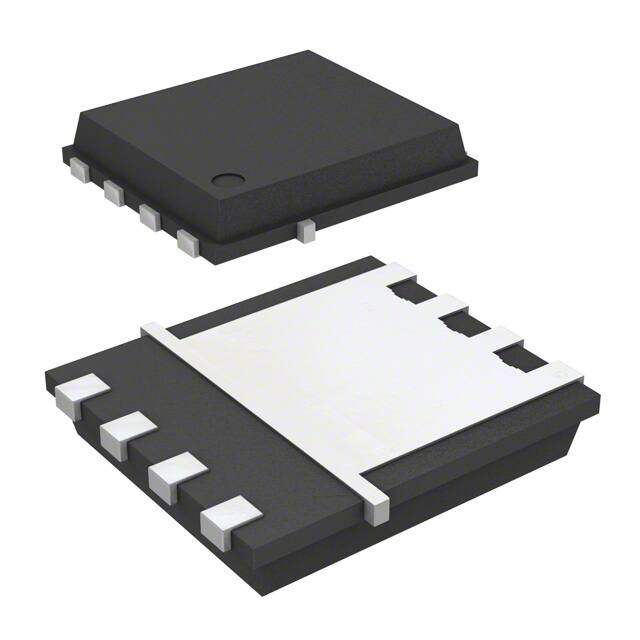
Package 8-PowerTDFN
Category Discrete Semiconductor Products / Transistors - FETs, MOSFETs - Single
Description
In a Pack of 5, N-Channel MOSFET, 100 A, 60 V, 8-Pin Power 56 ON Semiconductor FDMS030N06B
PDF
/
Buying Options
Total Price: USD $2.99
Unit Price: USD $2.992
≥1 USD $2.992
≥10 USD $2.51152
≥100 USD $2.031832
≥500 USD $1.806042
≥1000 USD $1.546424
Inventory: 1109
Minimum: 1
-
+

Technical Details
Compliance
Lead Free Lead Free
RoHS Status ROHS3 Compliant
Dimensions
Width 6.25mm
Length 5.1mm
Height 1.05mm
Technical
Pulsed Drain Current-Max (IDM) 400A
Drain to Source Breakdown Voltage 60V
Drain-source On Resistance-Max 0.003Ohm
Drain Current-Max (Abs) (ID) 22.1A
Gate to Source Voltage (Vgs) 20V
JEDEC-95 Code MO-240AA
Continuous Drain Current (ID) 100A
Turn-Off Delay Time 52 ns
Fall Time (Typ) 16 ns
Vgs (Max) ±20V
Drive Voltage (Max Rds On,Min Rds On) 10V
Rise Time 20 ns
Gate Charge (Qg) (Max) @ Vgs 75nC @ 10V
Current - Continuous Drain (Id) @ 25°C 22.1A Ta 100A Tc
Input Capacitance (Ciss) (Max) @ Vds 7560pF @ 30V
Vgs(th) (Max) @ Id 4.5V @ 250μA
Rds On (Max) @ Id, Vgs 3m Ω @ 50A, 10V
Transistor Application SWITCHING
FET Type N-Channel
Turn On Delay Time 39 ns
Case Connection DRAIN
Power Dissipation 104W
Operating Mode ENHANCEMENT MODE
Element Configuration Single
Power Dissipation-Max 2.5W Ta 104W Tc
Number of Elements 1
JESD-30 Code R-PDSO-F5
Time@Peak Reflow Temperature-Max (s) NOT SPECIFIED
Reach Compliance Code not_compliant
Peak Reflow Temperature (Cel) NOT SPECIFIED
Terminal Form FLAT
Terminal Position DUAL
Technology MOSFET (Metal Oxide)
Subcategory FET General Purpose Power
Terminal Finish Tin (Sn)
ECCN Code EAR99
Number of Terminations 5
Moisture Sensitivity Level (MSL) 1 (Unlimited)
Part Status Active
Pbfree Code yes
JESD-609 Code e3
Series PowerTrench?
Published 2013
Packaging Tape & Reel (TR)
Operating Temperature -55°C~150°C TJ
Physical
Transistor Element Material SILICON
Weight 68.1mg
Number of Pins 8
Package / Case 8-PowerTDFN
Mounting Type Surface Mount
Mount Surface Mount
Supply Chain
Lifecycle Status ACTIVE (Last Updated: 2 days ago)
Factory Lead Time 6 Weeks
Alternative Model

Recommended For You

FDMS030N06B+price,FDMS030N06B+datasheet,FDMS030N06B+in stock,buy+FDMS030N06B,finder+FDMS030N06B,FDMS030N06B+tutorials,FDMS030N06B+download