FDMA520PZ
RoHS  RoHS compliant
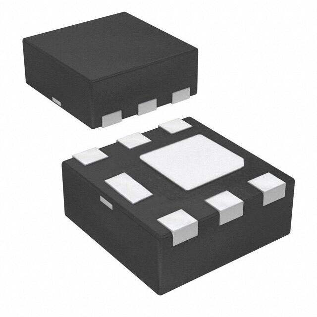
Package 6-VDFN Exposed Pad
Category Discrete Semiconductor Products / Transistors - FETs, MOSFETs - Single
Description
MOSFET -20V P-CH PowerTrench MOSFET
PDF
/
Buying Options
Total Price: USD $2.77
Unit Price: USD $2.76545
≥1 USD $2.76545
≥10 USD $2.26955
≥100 USD $2.1983
≥500 USD $2.12705
≥1000 USD $2.05675
Inventory: 35027
Minimum: 1
-
+

Technical Details
Compliance
Lead Free Lead Free
RoHS Status ROHS3 Compliant
REACH SVHC No SVHC
Dimensions
Width 2mm
Length 2mm
Height 750μm
Technical
Nominal Vgs -1.1 V
Dual Supply Voltage -20V
Pulsed Drain Current-Max (IDM) 24A
Drain to Source Breakdown Voltage -20V
Gate to Source Voltage (Vgs) 12V
Continuous Drain Current (ID) 7.3A
Turn-Off Delay Time 83 ns
Fall Time (Typ) 74 ns
Vgs (Max) ±12V
Drive Voltage (Max Rds On,Min Rds On) 2.5V 4.5V
Drain to Source Voltage (Vdss) 20V
Rise Time 29 ns
Gate Charge (Qg) (Max) @ Vgs 20nC @ 4.5V
Current - Continuous Drain (Id) @ 25°C 7.3A Ta
Input Capacitance (Ciss) (Max) @ Vds 1645pF @ 10V
Vgs(th) (Max) @ Id 1.5V @ 250μA
Rds On (Max) @ Id, Vgs 30m Ω @ 7.3A, 4.5V
FET Type P-Channel
Turn On Delay Time 10 ns
Power Dissipation 2.4W
Operating Mode ENHANCEMENT MODE
Element Configuration Single
Power Dissipation-Max 2.4W Ta
Number of Elements 1
Qualification Status Not Qualified
Time@Peak Reflow Temperature-Max (s) NOT SPECIFIED
Current Rating -7.3A
Peak Reflow Temperature (Cel) NOT SPECIFIED
Terminal Form NO LEAD
Terminal Position DUAL
Technology MOSFET (Metal Oxide)
Voltage - Rated DC -20V
Subcategory Other Transistors
Terminal Finish Nickel/Palladium/Gold (Ni/Pd/Au)
Resistance 30MOhm
ECCN Code EAR99
Termination SMD/SMT
Number of Terminations 6
Moisture Sensitivity Level (MSL) 1 (Unlimited)
Part Status Active
Pbfree Code yes
JESD-609 Code e4
Series PowerTrench?
Packaging Tape & Reel (TR)
Operating Temperature -55°C~150°C TJ
Physical
Transistor Element Material SILICON
Weight 30mg
Number of Pins 6
Package / Case 6-VDFN Exposed Pad
Mounting Type Surface Mount
Mount Surface Mount
Supply Chain
Lifecycle Status ACTIVE (Last Updated: 4 days ago)
Factory Lead Time 16 Weeks
Alternative Model

Recommended For You

FDMA520PZ+price,FDMA520PZ+datasheet,FDMA520PZ+in stock,buy+FDMA520PZ,finder+FDMA520PZ,FDMA520PZ+tutorials,FDMA520PZ+download