FDFME3N311ZT
RoHS
/
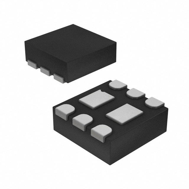
Package 6-UFDFN Exposed Pad
Category Discrete Semiconductor Products / Transistors - FETs, MOSFETs - Single
Description
MOSFET Int. NCh PowerTrench MOSFET & Sch. Diode
PDF
/
Buying Options
Total Price: USD $0.22
Unit Price: USD $0.22
≥1 USD $0.22
Inventory: 1095
Minimum: 1
-
+

Technical Details
Compliance
RoHS Status RoHS Compliant
REACH SVHC No SVHC
Radiation Hardening No
Dimensions
Width 1.6mm
Length 1.6mm
Height 550μm
Technical
Nominal Vgs 1 V
FET Feature Schottky Diode (Isolated)
Drain to Source Breakdown Voltage 30V
Drain-source On Resistance-Max 0.299Ohm
Gate to Source Voltage (Vgs) 12V
Threshold Voltage 1V
Continuous Drain Current (ID) 1.6A
Turn-Off Delay Time 22 ns
Fall Time (Typ) 2.8 ns
Vgs (Max) ±12V
Drive Voltage (Max Rds On,Min Rds On) 2.5V 4.5V
Rise Time 16 ns
Gate Charge (Qg) (Max) @ Vgs 1.4nC @ 4.5V
Current - Continuous Drain (Id) @ 25°C 1.8A Ta
Input Capacitance (Ciss) (Max) @ Vds 75pF @ 15V
Vgs(th) (Max) @ Id 1.5V @ 250μA
Rds On (Max) @ Id, Vgs 299m Ω @ 1.6A, 4.5V
Transistor Application SWITCHING
FET Type N-Channel
Turn On Delay Time 6 ns
Case Connection DRAIN
Power Dissipation 1.1W
Operating Mode ENHANCEMENT MODE
Element Configuration Single
Power Dissipation-Max 1.4W Ta
Number of Elements 1
Terminal Position DUAL
Technology MOSFET (Metal Oxide)
Subcategory FET General Purpose Power
Terminal Finish Nickel/Palladium/Gold (Ni/Pd/Au)
ECCN Code EAR99
Number of Terminations 6
Moisture Sensitivity Level (MSL) 1 (Unlimited)
Part Status Obsolete
Pbfree Code yes
JESD-609 Code e4
Series PowerTrench?
Published 2009
Packaging Tape & Reel (TR)
Operating Temperature -55°C~150°C TJ
Physical
Transistor Element Material SILICON
Weight 25.2mg
Number of Pins 6
Package / Case 6-UFDFN Exposed Pad
Mounting Type Surface Mount
Mount Surface Mount
Supply Chain
Lifecycle Status LAST SHIPMENTS (Last Updated: 1 week ago)
Alternative Model

Recommended For You

FDFME3N311ZT+price,FDFME3N311ZT+datasheet,FDFME3N311ZT+in stock,buy+FDFME3N311ZT,finder+FDFME3N311ZT,FDFME3N311ZT+tutorials,FDFME3N311ZT+download