FDD6296
RoHS  RoHS compliant
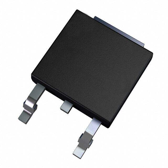
Package TO-252-3, DPak (2 Leads + Tab), SC-63
Category Discrete Semiconductor Products / Transistors - FETs, MOSFETs - Single
Description
Trans MOSFET N-CH 30V 15A 3-Pin(2+Tab) TO-252AA T/R
PDF
/
Buying Options
Total Price: USD $0.16
Unit Price: USD $0.1615
≥1 USD $0.1615
≥10 USD $0.13205
≥100 USD $0.12825
≥500 USD $0.12445
≥1000 USD $0.1197
≥10000 USD $0.10735
Inventory: 25807
Minimum: 1
-
+

Technical Details
Compliance
Lead Free Lead Free
RoHS Status ROHS3 Compliant
Radiation Hardening No
Technical
Drain to Source Breakdown Voltage 30V
Gate to Source Voltage (Vgs) 20V
Continuous Drain Current (ID) 50A
Turn-Off Delay Time 29 ns
Fall Time (Typ) 13 ns
Vgs (Max) ±20V
Drive Voltage (Max Rds On,Min Rds On) 4.5V 10V
Rise Time 6 ns
Gate Charge (Qg) (Max) @ Vgs 31.5nC @ 10V
Current - Continuous Drain (Id) @ 25°C 15A Ta 50A Tc
Input Capacitance (Ciss) (Max) @ Vds 1440pF @ 15V
Vgs(th) (Max) @ Id 3V @ 250μA
Rds On (Max) @ Id, Vgs 8.8m Ω @ 15A, 10V
Transistor Application SWITCHING
FET Type N-Channel
Turn On Delay Time 11 ns
Case Connection DRAIN
Power Dissipation 3.8W
Operating Mode ENHANCEMENT MODE
Element Configuration Single
Power Dissipation-Max 3.8W Ta 52W Tc
Number of Elements 1
JESD-30 Code R-PSSO-G2
Current Rating 50A
Terminal Form GULL WING
Technology MOSFET (Metal Oxide)
Voltage - Rated DC 30V
Subcategory FET General Purpose Power
Terminal Finish Tin (Sn)
Resistance 8.8MOhm
ECCN Code EAR99
Number of Terminations 2
Moisture Sensitivity Level (MSL) 1 (Unlimited)
Part Status Active
Pbfree Code yes
JESD-609 Code e3
Series PowerTrench?
Packaging Tape & Reel (TR)
Operating Temperature -55°C~175°C TJ
Physical
Transistor Element Material SILICON
Weight 260.37mg
Number of Pins 3
Package / Case TO-252-3, DPak (2 Leads + Tab), SC-63
Mounting Type Surface Mount
Mount Surface Mount
Supply Chain
Lifecycle Status ACTIVE (Last Updated: 14 hours ago)
Factory Lead Time 10 Weeks
Alternative Model

Recommended For You

FDD6296+price,FDD6296+datasheet,FDD6296+in stock,buy+FDD6296,finder+FDD6296,FDD6296+tutorials,FDD6296+download