FDD3672
RoHS  RoHS compliant
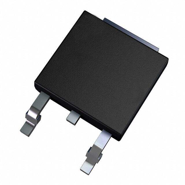
Package TO-252-3, DPak (2 Leads + Tab), SC-63
Category Discrete Semiconductor Products / Transistors - FETs, MOSFETs - Single
Description
MOSFET N-CH 100V 44A D-PAK
PDF
/
Buying Options
Total Price: USD $1.43
Unit Price: USD $1.4344
≥1 USD $1.4344
≥10 USD $1.18888
≥100 USD $0.946176
≥500 USD $0.800571
≥1000 USD $0.679272
Inventory: 1317
Minimum: 1
-
+

Technical Details
Compliance
Lead Free Lead Free
RoHS Status ROHS3 Compliant
REACH SVHC No SVHC
Dimensions
Width 5.59mm
Length 6.73mm
Height 2.39mm
Technical
Nominal Vgs 4 V
Dual Supply Voltage 100V
Drain to Source Breakdown Voltage 100V
Drain Current-Max (Abs) (ID) 6.5A
Gate to Source Voltage (Vgs) 20V
JEDEC-95 Code TO-252AA
Threshold Voltage 4V
Continuous Drain Current (ID) 44A
Turn-Off Delay Time 26 ns
Fall Time (Typ) 44 ns
Vgs (Max) ±20V
Drive Voltage (Max Rds On,Min Rds On) 6V 10V
Rise Time 59 ns
Gate Charge (Qg) (Max) @ Vgs 36nC @ 10V
Current - Continuous Drain (Id) @ 25°C 6.5A Ta 44A Tc
Input Capacitance (Ciss) (Max) @ Vds 1710pF @ 25V
Vgs(th) (Max) @ Id 4V @ 250μA
Rds On (Max) @ Id, Vgs 28m Ω @ 44A, 10V
Transistor Application SWITCHING
FET Type N-Channel
Turn On Delay Time 11 ns
Case Connection DRAIN
Power Dissipation 135W
Operating Mode ENHANCEMENT MODE
Element Configuration Single
Power Dissipation-Max 135W Tc
Number of Elements 1
Qualification Status Not Qualified
JESD-30 Code R-PSSO-G2
Time@Peak Reflow Temperature-Max (s) NOT SPECIFIED
Current Rating 44A
Reach Compliance Code not_compliant
Peak Reflow Temperature (Cel) NOT SPECIFIED
Terminal Form GULL WING
Technology MOSFET (Metal Oxide)
Voltage - Rated DC 100V
Subcategory FET General Purpose Power
Resistance 28MOhm
ECCN Code EAR99
Termination SMD/SMT
Number of Terminations 2
Moisture Sensitivity Level (MSL) 1 (Unlimited)
Part Status Active
Pbfree Code yes
JESD-609 Code e3
Series UltraFET?
Published 2002
Packaging Tape & Reel (TR)
Operating Temperature -55°C~175°C TJ
Physical
Transistor Element Material SILICON
Weight 260.37mg
Number of Pins 3
Package / Case TO-252-3, DPak (2 Leads + Tab), SC-63
Mounting Type Surface Mount
Mount Surface Mount
Contact Plating Tin
Supply Chain
Lifecycle Status ACTIVE (Last Updated: 1 week ago)
Factory Lead Time 8 Weeks
Alternative Model

Recommended For You

FDD3672+price,FDD3672+datasheet,FDD3672+in stock,buy+FDD3672,finder+FDD3672,FDD3672+tutorials,FDD3672+download