ECH8419-TL-H
RoHS
/
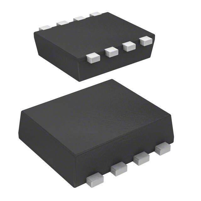
Package 8-SMD, Flat Lead
Category Discrete Semiconductor Products / Transistors - FETs, MOSFETs - Single
Description
Tape & Reel (TR) Surface Mount N-Channel Single Mosfet Transistor 9A Ta 9A 1.5W Ta 31ns
PDF
/
Buying Options
Total Price: USD $0.47
Unit Price: USD $0.473143
≥1 USD $0.473143
≥10 USD $0.446363
≥100 USD $0.421101
≥500 USD $0.397266
≥1000 USD $0.374777
Inventory: 1113
Minimum: 1
-
+

Technical Details
Compliance
Lead Free Lead Free
RoHS Status RoHS Compliant
Radiation Hardening No
Dimensions
Width 2.3mm
Length 2.9mm
Height 900μm
Technical
Drain to Source Breakdown Voltage 35V
Drain Current-Max (Abs) (ID) 9A
Gate to Source Voltage (Vgs) 20V
Continuous Drain Current (ID) 9A
Turn-Off Delay Time 66 ns
Fall Time (Typ) 31 ns
Vgs (Max) ±20V
Drive Voltage (Max Rds On,Min Rds On) 4V 10V
Rise Time 26ns
Gate Charge (Qg) (Max) @ Vgs 19nC @ 10V
Current - Continuous Drain (Id) @ 25°C 9A Ta
Input Capacitance (Ciss) (Max) @ Vds 960pF @ 20V
Halogen Free Halogen Free
Vgs(th) (Max) @ Id 2.6V @ 1mA
Rds On (Max) @ Id, Vgs 17m Ω @ 5A, 10V
FET Type N-Channel
Turn On Delay Time 13 ns
Element Configuration Single
Power Dissipation-Max 1.5W Ta
Pin Count 8
Technology MOSFET (Metal Oxide)
Subcategory FET General Purpose Powers
Terminal Finish Tin/Bismuth (Sn/Bi)
ECCN Code EAR99
Moisture Sensitivity Level (MSL) 1 (Unlimited)
Part Status Obsolete
Pbfree Code yes
JESD-609 Code e6
Published 2012
Packaging Tape & Reel (TR)
Operating Temperature 150°C TJ
Physical
Number of Pins 8
Surface Mount YES
Package / Case 8-SMD, Flat Lead
Mounting Type Surface Mount
Recommended For You

ECH8419-TL-H+price,ECH8419-TL-H+datasheet,ECH8419-TL-H+in stock,buy+ECH8419-TL-H,finder+ECH8419-TL-H,ECH8419-TL-H+tutorials,ECH8419-TL-H+download