CPH6337-TL-E
RoHS
/
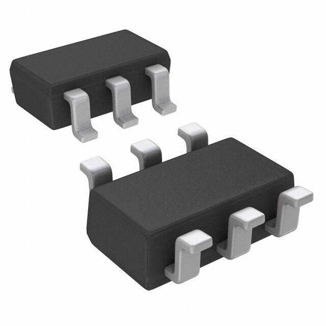
Package SOT-23-6 Thin, TSOT-23-6
Category Discrete Semiconductor Products / Transistors - FETs, MOSFETs - Single
Description
Tape & Reel (TR) Surface Mount P-Channel Single Mosfet Transistor 3.5A Ta 3.5A 1.6W 50ns
PDF
/
Buying Options
Total Price: USD $1.34
Unit Price: USD $1.3395
≥1 USD $1.3395
≥10 USD $1.09915
≥100 USD $1.06495
≥500 USD $1.03075
≥1000 USD $0.99655
Inventory: 13259
Minimum: 1
-
+

Technical Details
Compliance
Lead Free Lead Free
RoHS Status RoHS Compliant
Dimensions
Width 1.6mm
Length 2.9mm
Height 900μm
Technical
Drain to Source Breakdown Voltage 12V
Gate to Source Voltage (Vgs) 10V
Continuous Drain Current (ID) 3.5A
Turn-Off Delay Time 41 ns
Fall Time (Typ) 50 ns
Vgs (Max) ±10V
Drive Voltage (Max Rds On,Min Rds On) 1.8V 4.5V
Rise Time 80ns
Gate Charge (Qg) (Max) @ Vgs 5.6nC @ 4.5V
Current - Continuous Drain (Id) @ 25°C 3.5A Ta
Input Capacitance (Ciss) (Max) @ Vds 405pF @ 6V
Vgs(th) (Max) @ Id 1.4V @ 1mA
Rds On (Max) @ Id, Vgs 70m Ω @ 1.5A, 4.5V
FET Type P-Channel
Turn On Delay Time 8.8 ns
Power Dissipation 1.6W
Element Configuration Single
Power Dissipation-Max 1.6W Ta
Pin Count 6
Technology MOSFET (Metal Oxide)
Subcategory Other Transistors
Terminal Finish Tin/Bismuth (Sn/Bi)
Resistance 70mOhm
ECCN Code EAR99
Moisture Sensitivity Level (MSL) 1 (Unlimited)
Part Status Obsolete
Pbfree Code yes
JESD-609 Code e6
Published 2012
Packaging Tape & Reel (TR)
Operating Temperature 150°C TJ
Physical
Number of Pins 6
Surface Mount YES
Package / Case SOT-23-6 Thin, TSOT-23-6
Mounting Type Surface Mount
Recommended For You

CPH6337-TL-E+price,CPH6337-TL-E+datasheet,CPH6337-TL-E+in stock,buy+CPH6337-TL-E,finder+CPH6337-TL-E,CPH6337-TL-E+tutorials,CPH6337-TL-E+download