CPH3348-TL-E
RoHS
/
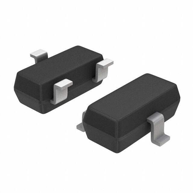
Package SC-96
Category Discrete Semiconductor Products / Transistors - FETs, MOSFETs - Single
Description
MOSFET P-CH 12V 3A CPH3
PDF
/
Buying Options
Total Price: USD $0.18
Unit Price: USD $0.176
≥1 USD $0.176
Inventory: 1584
Minimum: 1
-
+

Technical Details
Compliance
Lead Free Lead Free
RoHS Status RoHS Compliant
Dimensions
Width 1.6mm
Length 2.9mm
Height 900μm
Technical
Drain to Source Breakdown Voltage 12V
Drain Current-Max (Abs) (ID) 3A
Gate to Source Voltage (Vgs) 10V
Continuous Drain Current (ID) 3A
Turn-Off Delay Time 41 ns
Fall Time (Typ) 50 ns
Vgs (Max) ±10V
Drive Voltage (Max Rds On,Min Rds On) 1.8V 4.5V
Rise Time 80 ns
Gate Charge (Qg) (Max) @ Vgs 5.6nC @ 4.5V
Current - Continuous Drain (Id) @ 25°C 3A Ta
Input Capacitance (Ciss) (Max) @ Vds 405pF @ 6V
Rds On (Max) @ Id, Vgs 70m Ω @ 1.5A, 4.5V
Transistor Application SWITCHING
FET Type P-Channel
Turn On Delay Time 8.8 ns
Power Dissipation 1W
Operating Mode ENHANCEMENT MODE
Element Configuration Single
Power Dissipation-Max 1W Ta
Number of Elements 1
Pin Count 3
Terminal Form GULL WING
Terminal Position DUAL
Technology MOSFET (Metal Oxide)
Subcategory Other Transistors
Resistance 70mOhm
ECCN Code EAR99
Number of Terminations 3
Moisture Sensitivity Level (MSL) 1 (Unlimited)
Part Status Obsolete
Pbfree Code yes
JESD-609 Code e6
Published 2007
Packaging Tape & Reel (TR)
Operating Temperature 150°C TJ
Physical
Transistor Element Material SILICON
Number of Pins 3
Surface Mount YES
Package / Case SC-96
Mounting Type Surface Mount
Contact Plating Tin
Alternative Model

Recommended For You

CPH3348-TL-E+price,CPH3348-TL-E+datasheet,CPH3348-TL-E+in stock,buy+CPH3348-TL-E,finder+CPH3348-TL-E,CPH3348-TL-E+tutorials,CPH3348-TL-E+download