BVSS84LT1G
RoHS  RoHS compliant
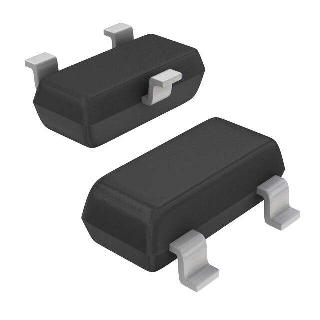
Package TO-236-3, SC-59, SOT-23-3
Category Discrete Semiconductor Products / Transistors - FETs, MOSFETs - Single
Description
Trans MOSFET P-CH 50V 0.13A Automotive 3-Pin SOT-23 T/R
PDF
/
Buying Options
Total Price: USD $0.27
Unit Price: USD $0.2698
≥1 USD $0.2698
≥10 USD $0.22135
≥100 USD $0.2147
≥500 USD $0.20805
≥1000 USD $0.20045
≥10000 USD $0.17955
Inventory: 191887
Minimum: 1
-
+

Technical Details
Compliance
Lead Free Lead Free
RoHS Status ROHS3 Compliant
Radiation Hardening No
Technical
Drain to Source Breakdown Voltage -50V
Gate to Source Voltage (Vgs) 20V
Continuous Drain Current (ID) 130mA
Turn-Off Delay Time 12 ns
Fall Time (Typ) 1.7 ns
Vgs (Max) ±20V
Drive Voltage (Max Rds On,Min Rds On) 5V
Drain to Source Voltage (Vdss) 50V
Rise Time 9.7 ns
Gate Charge (Qg) (Max) @ Vgs 2.2nC @ 10V
Current - Continuous Drain (Id) @ 25°C 130mA Ta
Input Capacitance (Ciss) (Max) @ Vds 36pF @ 5V
Halogen Free Halogen Free
Vgs(th) (Max) @ Id 2V @ 250μA
Rds On (Max) @ Id, Vgs 10 Ω @ 100mA, 5V
FET Type P-Channel
Turn On Delay Time 3.6 ns
Power Dissipation 225mW
Operating Mode ENHANCEMENT MODE
Element Configuration Single
Power Dissipation-Max 225mW Ta
Number of Channels 1
Number of Elements 1
Pin Count 3
Time@Peak Reflow Temperature-Max (s) 10
Peak Reflow Temperature (Cel) 260
Terminal Form GULL WING
Terminal Position DUAL
Technology MOSFET (Metal Oxide)
Subcategory Other Transistors
Terminal Finish Tin (Sn)
ECCN Code EAR99
Number of Terminations 3
Moisture Sensitivity Level (MSL) 1 (Unlimited)
Part Status Active
Pbfree Code yes
JESD-609 Code e3
Published 2004
Packaging Tape & Reel (TR)
Operating Temperature -55°C~150°C TJ
Physical
Transistor Element Material SILICON
Weight 1.437803g
Number of Pins 3
Surface Mount YES
Package / Case TO-236-3, SC-59, SOT-23-3
Mounting Type Surface Mount
Supply Chain
Lifecycle Status ACTIVE (Last Updated: 2 days ago)
Factory Lead Time 4 Weeks
Alternative Model

Recommended For You

BVSS84LT1G+price,BVSS84LT1G+datasheet,BVSS84LT1G+in stock,buy+BVSS84LT1G,finder+BVSS84LT1G,BVSS84LT1G+tutorials,BVSS84LT1G+download