BS170RLRP
RoHS
/
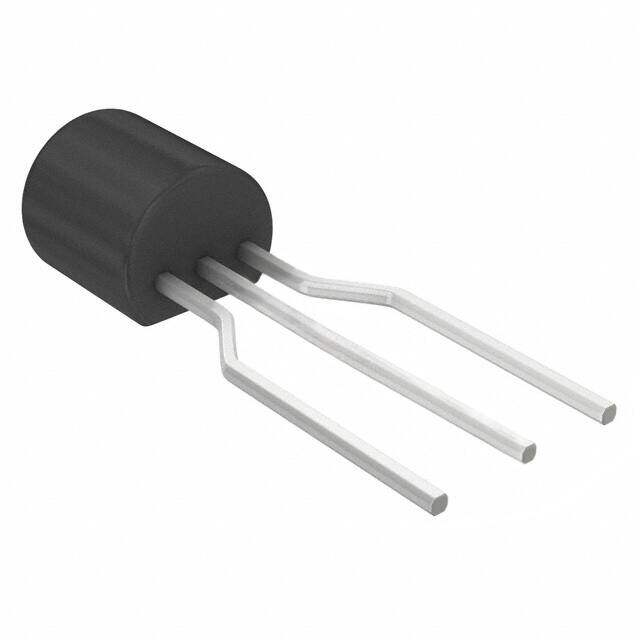
Package TO-226-3, TO-92-3 (TO-226AA) (Formed Leads)
Category Discrete Semiconductor Products / Transistors - FETs, MOSFETs - Single
Description
MOSFET N-CH 60V 500MA TO-92
PDF
/
Inventory: 9831
Minimum: /
The more specific your information, the faster response you will get.
Please complete the following form with the details of your request part and
contact information to get a quote.
Quotation Consultation
Technical Details
Compliance
Lead Free Contains Lead
RoHS Status Non-RoHS Compliant
Technical
Drain to Source Breakdown Voltage 60V
Drain-source On Resistance-Max 5Ohm
Drain Current-Max (Abs) (ID) 0.5A
Gate to Source Voltage (Vgs) 20V
Continuous Drain Current (ID) 500mA
Vgs (Max) ±20V
Drive Voltage (Max Rds On,Min Rds On) 10V
Current - Continuous Drain (Id) @ 25°C 500mA Ta
Input Capacitance (Ciss) (Max) @ Vds 60pF @ 10V
Vgs(th) (Max) @ Id 3V @ 1mA
Rds On (Max) @ Id, Vgs 5 Ω @ 200mA, 10V
Transistor Application SWITCHING
FET Type N-Channel
Power Dissipation 350mW
Operating Mode ENHANCEMENT MODE
Element Configuration Single
Power Dissipation-Max 350mW Ta
Number of Elements 1
Qualification Status Not Qualified
JESD-30 Code O-PBCY-T3
Pin Count 3
Time@Peak Reflow Temperature-Max (s) 30
Current Rating 500mA
Reach Compliance Code not_compliant
Peak Reflow Temperature (Cel) 240
Terminal Position BOTTOM
Technology MOSFET (Metal Oxide)
Voltage - Rated DC 60V
Subcategory FET General Purpose Power
HTS Code 8541.21.00.95
Terminal Finish Tin/Lead (Sn/Pb)
ECCN Code EAR99
Number of Terminations 3
Moisture Sensitivity Level (MSL) 1 (Unlimited)
Part Status Obsolete
JESD-609 Code e0
Published 2005
Packaging Tape & Box (TB)
Operating Temperature -55°C~150°C TJ
Physical
Transistor Element Material SILICON
Package / Case TO-226-3, TO-92-3 (TO-226AA) (Formed Leads)
Mounting Type Through Hole
Mount Through Hole
Alternative Model

Recommended For You

BS170RLRP+price,BS170RLRP+datasheet,BS170RLRP+in stock,buy+BS170RLRP,finder+BS170RLRP,BS170RLRP+tutorials,BS170RLRP+download