BS107G
RoHS
/
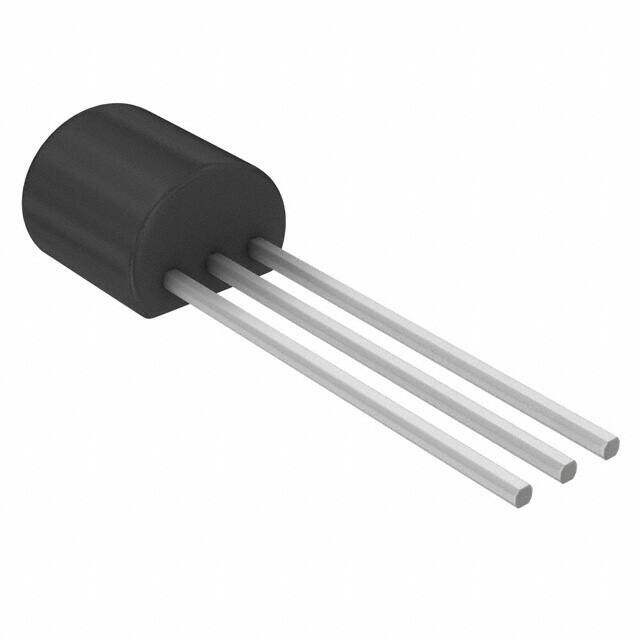
Package TO-226-3, TO-92-3 (TO-226AA)
Category Discrete Semiconductor Products / Transistors - FETs, MOSFETs - Single
Description
MOSFET N-CH 200V 0.25A TO-92
PDF
/
Buying Options
Total Price: USD $25.49
Unit Price: USD $25.4942
≥1 USD $25.4942
≥10 USD $20.91805
≥100 USD $20.26445
≥500 USD $19.61085
≥1000 USD $18.95725
Inventory: 1150
Minimum: 1
-
+

Technical Details
Compliance
Lead Free Lead Free
RoHS Status RoHS Compliant
Technical
Drain to Source Breakdown Voltage 200V
Drain Current-Max (Abs) (ID) 0.25A
Gate to Source Voltage (Vgs) 20V
Threshold Voltage 3V
Continuous Drain Current (ID) 250mA
Vgs (Max) ±20V
Drive Voltage (Max Rds On,Min Rds On) 2.6V 10V
Current - Continuous Drain (Id) @ 25°C 250mA Ta
Input Capacitance (Ciss) (Max) @ Vds 60pF @ 25V
Vgs(th) (Max) @ Id 3V @ 1mA
Rds On (Max) @ Id, Vgs 14 Ω @ 200mA, 10V
Transistor Application SWITCHING
FET Type N-Channel
Power Dissipation 350mW
Operating Mode ENHANCEMENT MODE
Element Configuration Single
Power Dissipation-Max 350mW Ta
Number of Elements 1
Qualification Status Not Qualified
Pin Count 3
Time@Peak Reflow Temperature-Max (s) 40
Current Rating 250mA
Peak Reflow Temperature (Cel) 260
Terminal Position BOTTOM
Technology MOSFET (Metal Oxide)
Voltage - Rated DC 200V
Subcategory FET General Purpose Power
Terminal Finish Tin/Silver/Copper (Sn/Ag/Cu)
ECCN Code EAR99
Number of Terminations 3
Moisture Sensitivity Level (MSL) 1 (Unlimited)
Part Status Obsolete
Pbfree Code yes
JESD-609 Code e1
Published 2007
Packaging Bulk
Operating Temperature -55°C~150°C TJ
Physical
Transistor Element Material SILICON
Number of Pins 3
Package / Case TO-226-3, TO-92-3 (TO-226AA)
Mounting Type Through Hole
Mount Through Hole
Contact Plating Copper, Silver, Tin
Supply Chain
Lifecycle Status LAST SHIPMENTS (Last Updated: 1 week ago)
Alternative Model

Recommended For You

BS107G+price,BS107G+datasheet,BS107G+in stock,buy+BS107G,finder+BS107G,BS107G+tutorials,BS107G+download