2SK3816-DL-E
RoHS
/
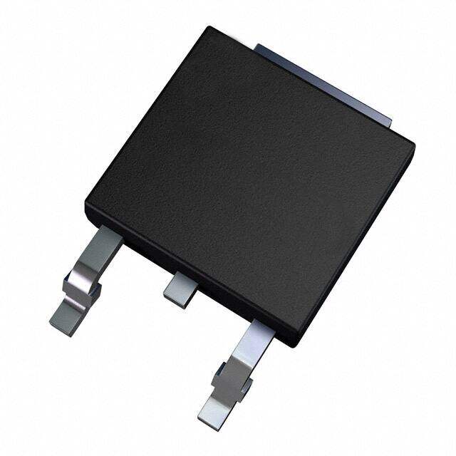
Package TO-252-3, DPak (2 Leads + Tab), SC-63
Category Discrete Semiconductor Products / Transistors - FETs, MOSFETs - Single
Description
MOSFET N-CH 60V 40A SMP-FD
PDF
/
Buying Options
Total Price: USD $0.94
Unit Price: USD $0.9405
≥1 USD $0.9405
≥10 USD $0.7714
≥100 USD $0.74765
≥500 USD $0.72295
≥1000 USD $0.6992
Inventory: 1179
Minimum: 1
-
+

Technical Details
Compliance
RoHS Status RoHS Compliant
Radiation Hardening No
Technical
Gate to Source Voltage (Vgs) 20V
Continuous Drain Current (ID) 40A
Turn-Off Delay Time 160 ns
Fall Time (Typ) 160 ns
Vgs (Max) ±20V
Drive Voltage (Max Rds On,Min Rds On) 4V 10V
Drain to Source Voltage (Vdss) 60V
Rise Time 160ns
Gate Charge (Qg) (Max) @ Vgs 40nC @ 10V
Current - Continuous Drain (Id) @ 25°C 40A Ta
Input Capacitance (Ciss) (Max) @ Vds 1780pF @ 20V
Vgs(th) (Max) @ Id 2.6V @ 1mA
Rds On (Max) @ Id, Vgs 26m Ω @ 20A, 10V
FET Type N-Channel
Turn On Delay Time 16.5 ns
Power Dissipation 50W
Operating Mode ENHANCEMENT MODE
Power Dissipation-Max 1.65W Ta 50W Tc
Configuration Single
Technology MOSFET (Metal Oxide)
Subcategory FET General Purpose Power
Terminal Finish Tin/Bismuth (Sn/Bi)
Moisture Sensitivity Level (MSL) 1 (Unlimited)
Part Status Obsolete
JESD-609 Code e6
Published 2004
Packaging Tape & Reel (TR)
Operating Temperature 150°C TJ
Physical
Number of Pins 3
Package / Case TO-252-3, DPak (2 Leads + Tab), SC-63
Mounting Type Surface Mount
Mount Surface Mount
Alternative Model

Recommended For You

2SK3816-DL-E+price,2SK3816-DL-E+datasheet,2SK3816-DL-E+in stock,buy+2SK3816-DL-E,finder+2SK3816-DL-E,2SK3816-DL-E+tutorials,2SK3816-DL-E+download