1HP04CH-TL-W
RoHS  RoHS compliant
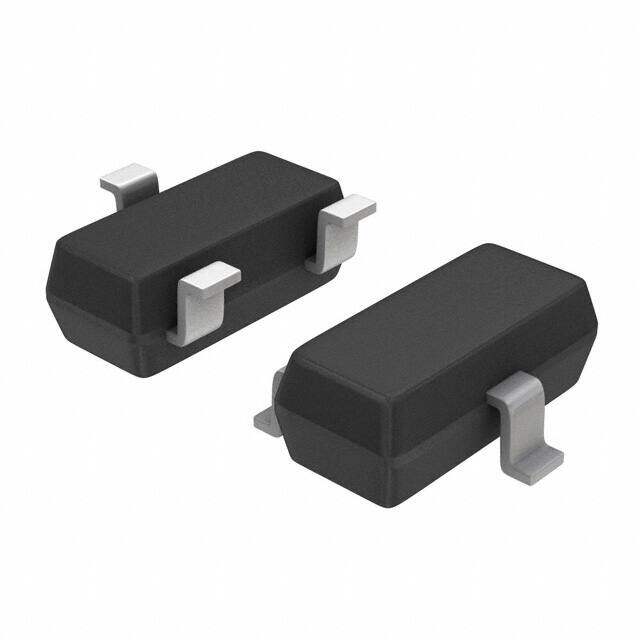
Package TO-236-3, SC-59, SOT-23-3
Category Discrete Semiconductor Products / Transistors - FETs, MOSFETs - Single
Description
MOSFET P-CH 100V 0.17A SOT-23
PDF
/
Buying Options
Total Price: USD $1.24
Unit Price: USD $1.2445
≥1 USD $1.2445
≥10 USD $1.02125
≥100 USD $0.9899
≥500 USD $0.9576
≥1000 USD $0.9253
Inventory: 90002
Minimum: 1
-
+

Technical Details
Compliance
Lead Free Lead Free
RoHS Status ROHS3 Compliant
Technical
Drain to Source Breakdown Voltage -100V
Gate to Source Voltage (Vgs) 20V
Continuous Drain Current (ID) 170mA
Turn-Off Delay Time 200 ns
Fall Time (Typ) 81 ns
Vgs (Max) ±20V
Drive Voltage (Max Rds On,Min Rds On) 4V 10V
Drain to Source Voltage (Vdss) 100V
Rise Time 18ns
Gate Charge (Qg) (Max) @ Vgs 0.9nC @ 10V
Current - Continuous Drain (Id) @ 25°C 170mA Ta
Input Capacitance (Ciss) (Max) @ Vds 14pF @ 20V
Vgs(th) (Max) @ Id 2.6V @ 100μA
Rds On (Max) @ Id, Vgs 18 Ω @ 80mA, 10V
Transistor Application SWITCHING
FET Type P-Channel
Turn On Delay Time 21 ns
Operating Mode ENHANCEMENT MODE
Number of Channels 1
Configuration SINGLE WITH BUILT-IN DIODE AND RESISTOR
Number of Elements 1
JESD-30 Code R-PDSO-G3
Terminal Form GULL WING
Terminal Position DUAL
Technology MOSFET (Metal Oxide)
Max Power Dissipation 600mW
Subcategory Other Transistors
ECCN Code EAR99
Number of Terminations 3
Moisture Sensitivity Level (MSL) 1 (Unlimited)
Part Status Active
Pbfree Code yes
JESD-609 Code e6
Published 2011
Packaging Tape & Reel (TR)
Operating Temperature 150°C TJ
Physical
Transistor Element Material SILICON
Package / Case TO-236-3, SC-59, SOT-23-3
Mounting Type Surface Mount
Mount Surface Mount
Contact Plating Tin
Supply Chain
Lifecycle Status ACTIVE (Last Updated: 21 hours ago)
Factory Lead Time 10 Weeks
Alternative Model

Recommended For You

1HP04CH-TL-W+price,1HP04CH-TL-W+datasheet,1HP04CH-TL-W+in stock,buy+1HP04CH-TL-W,finder+1HP04CH-TL-W,1HP04CH-TL-W+tutorials,1HP04CH-TL-W+download